Method for hiding a refresh in a pseudo-static memory

a pseudo-static memory and refresh technology, applied in memory adressing/allocation/relocation, digital storage, instruments, etc., can solve the disadvantages of disadvantageous data loss, disadvantageous array cycle time of drams, and complicated design of external memory controllers

Inactive Publication Date: 2006-08-01
INTELLECTUAL VENTURES I LLC
View PDF29 Cites 7 Cited by
  • Summary
  • Abstract
  • Description
  • Claims
  • Application Information

AI Technical Summary

Benefits of technology

[0006]This object and other advantageous effects are achieved using a pseudo-static memory device that substantially hides all refresh operations from a memory controller coupled to the pseudo-static memory device. In a first embodiment, such a device internally includes a set of DRAM sub-arrays (matrices) each having plural array rows, such that at least one row in one sub-array can be refreshed while responding to an access request in another sub-array. In a second embodiment, at least one non-array row (e.g., an SRAM row or a register), external to a set of DRAM sub-arrays, is used to allow a refresh of at least one row of its corresponding sub-array when the internal controller, as opposed to an external controller, determines that a refresh would be appropriate. The at least one non-array row may either be either direct mapped or fully associative, and the size of the non-array row may be smaller than, larger than, or equal to the size of each of the plural array rows.

Problems solved by technology

On the other hand, DRAM is disadvantageously prone to data loss if the individual rows of data are not periodically refreshed.
External circuitry complicates the design of an external memory controller and may therefore be disadvantageous.
DRAMs disadvantageously have relatively long array cycle times as compared to other memory devices (e.g., static memories) and therefore may act as a bottleneck for a processor that requests memory more quickly than the DRAM can provide it.
Unfortunately, the cost of SRAMs per bit is significantly more expensive than the cost of DRAMs per bit.
Accordingly, it is often prohibitively expensive to use SRAM for a computer's main memory, and instead a small amount of SRAM is used only for a memory cache between the processor and a larger amount of DRAM.
This characteristic requires the use of a memory controller that understands the operation of EDRAM devices and, thus, disadvantageously includes the additional circuitry for initiating those refresh cycles.

Method used


Image

  • Method for hiding a refresh in a pseudo-static memory
  • Method for hiding a refresh in a pseudo-static memory
  • Method for hiding a refresh in a pseudo-static memory

Examples


first embodiment

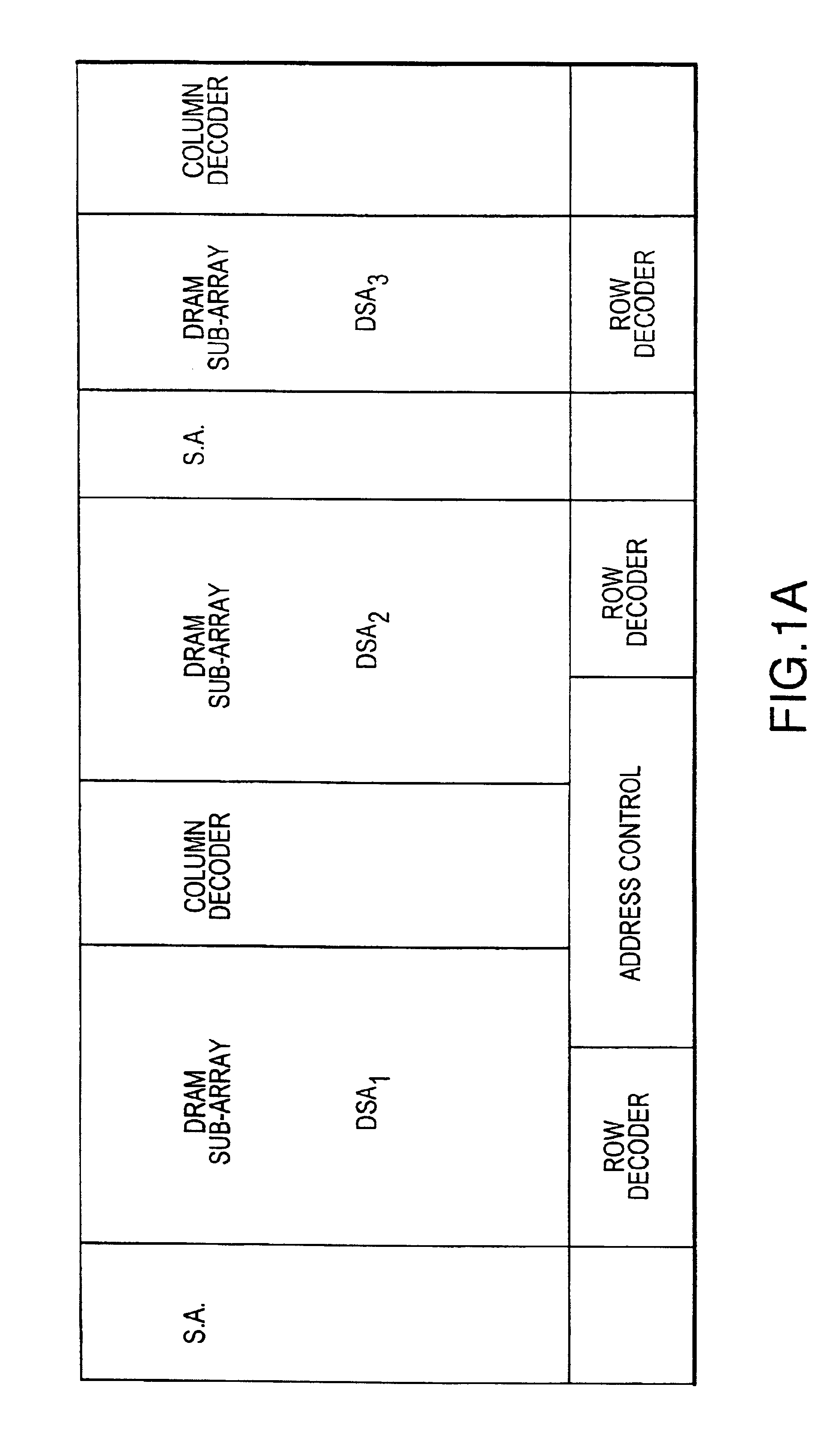
[0018]Referring now to the drawings, in which like reference numerals designate identical or corresponding parts throughout the several views, FIG. 1A is an illustration of a pseudo-static memory architecture according to a first aspect of the present invention. Generally, the present invention includes control circuitry for performing a refresh operation in at least a first DRAM sub-array when a second DRAM sub-array is being accessed (for reading or writing).

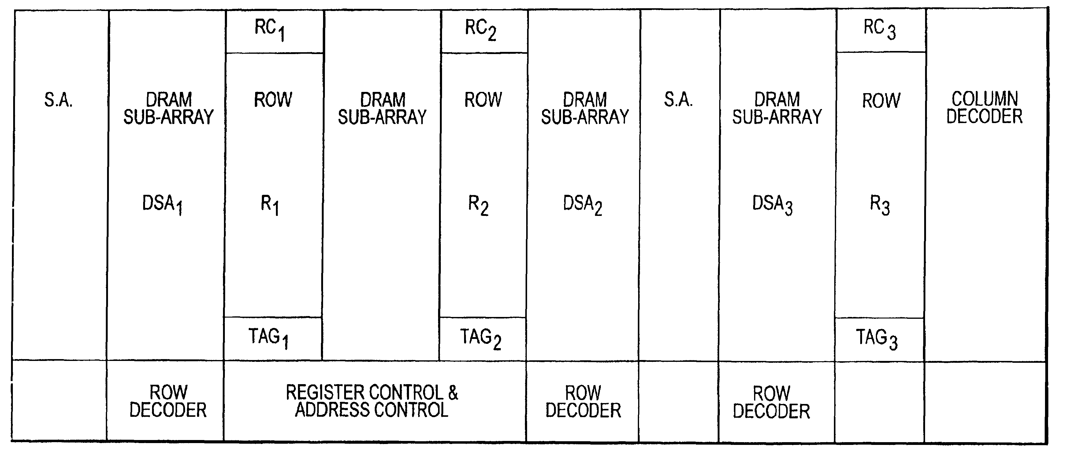
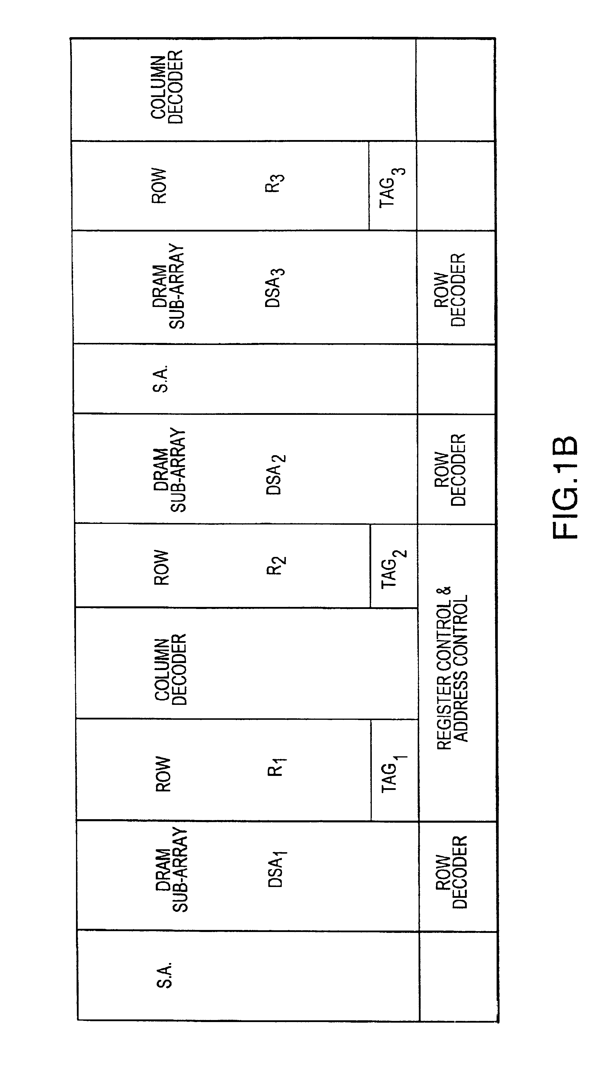
[0019]Turning now to FIG. 1B, in the second aspect, like the memory architecture shown in FIG. 7 of the '317 patent, a pseudo-static memory device includes both plural DRAM sub-arrays and at least one row (e.g., an SRAM row) coupled to the plural DRAM sub-arrays. The at least one row can act as an intermediate storage area for at least one of the plural DRAM sub-arrays when reading from or writing to that sub-array while contemporaneously refreshing a different DRAM sub-array.

[0020]For example, as illustrated in FIG. 2, a read...

second embodiment

[0022]The approach illustrated in FIG. 2, however, may adversely waste power by running refreshes excessively often. Consequently, in the present invention shown in FIG. 3, the pseudo-static memory device determines whether or not an appropriate amount of time has elapsed since the last refresh cycle. A refresh cycle is run behind the given access cycle only if the time has expired. As shown in FIG. 3, consecutive read misses occur for rows 1-4 of DSA1, thereby updating R1 and LRR1 after each miss. Unlike the timing diagram of FIG. 2, on the first read miss, a refresh cycle of at least one other sub-array does not occur since the timer has not yet decremented to zero. Instead, each clock cycle (either internal or external) the timer is decremented, thus RC(global) remains constant until the timer hits zero. In one implementation, the rollover of the counter sets a “refresh pending” flag, and the timer is allowed to decrement again immediately. In an alternate implementation, the tim...

fourth embodiment

[0025]It should be noted that the ability to hide a refresh cycle behind an access is contingent upon the ability to have the refresh cycle occur for an address in a different DRAM sub-array than the sub-array where the access is occurring. However, if a series of accesses are directed to a first DRAM sub-array, then the other sub-arrays are being refreshed properly, but the first sub-array is not. Accordingly, as shown in FIG. 5, the present invention includes separate refresh counters for each sub-array. This prevents a row in the first sub-array from being “skipped” when the corresponding row is refreshed in the other sub-arrays. As shown in FIG. 6, when a read miss occurs in DSA1, refreshes in DSA2 and DSA3 are performed and their corresponding refresh counters (i.e., RC2 and RC3) are updated. However, the value stored in RC1 is left unchanged, so that no rows in DSA1 are skipped for refresh.


PUM


Abstract

A method and device for hiding refresh operations during accesses to sub-arrays of a pseudo-static memory device. By refreshing sub-arrayj while filling the row Ri (where i≠j) corresponding to sub-arrayi, refresh operations can be performed without risking that a read request will interrupt the refresh operation. Additional refresh operations of sub-arrayi can be performed serially with the operations of filling the row Ri without delaying the overall burst read or write operation if the burst is made sufficiently long.

Description

FIELD OF THE INVENTION[0001]A method and system for hiding, from an external memory controller, a refresh operation (or plural refresh operations) in a pseudo-static memory device.BACKGROUND OF THE INVENTION[0002]A variety of memory devices are presently available with varying characteristics. Dynamic Random Access Memory (DRAM) has the advantage that the number of gates per cell is small and the density is generally quite high. On the other hand, DRAM is disadvantageously prone to data loss if the individual rows of data are not periodically refreshed. Accordingly, known systems have used external or internal refresh circuitry to prevent data loss. External circuitry complicates the design of an external memory controller and may therefore be disadvantageous. DRAMs disadvantageously have relatively long array cycle times as compared to other memory devices (e.g., static memories) and therefore may act as a bottleneck for a processor that requests memory more quickly than the DRAM c...

Claims


Application Information

Patent Timeline
Patent Type & Authority Patents(United States)
IPC IPC(8): G11C7/00G11C11/406
CPCG11C11/406G11C11/40615G11C11/40607G11C2211/4061
Inventor MOBLEY, KENNETH J.
Owner INTELLECTUAL VENTURES I LLC
Why Eureka
Try Eureka