Signal transmission circuit and method for equalizing disparate delay times dynamically, and data latch circuit of semiconductor device implementing the same

Inactive Publication Date: 2006-08-01
SAMSUNG ELECTRONICS CO LTD
View PDF11 Cites 81 Cited by
  • Summary
  • Abstract
  • Description
  • Claims
  • Application Information

AI Technical Summary

Benefits of technology

[0014]In the preferred embodiment, the auxiliary signal transmission path is a replica of the second transmission path. Accordingly, the third delay is always identical to the second delay, notwithstanding the parameters that introduce v

Problems solved by technology

The controllable delay unit receives the output from the second path, and further delays it by its internal delay to match

Method used


Image

  • Signal transmission circuit and method for equalizing disparate delay times dynamically, and data latch circuit of semiconductor device implementing the same
  • Signal transmission circuit and method for equalizing disparate delay times dynamically, and data latch circuit of semiconductor device implementing the same
  • Signal transmission circuit and method for equalizing disparate delay times dynamically, and data latch circuit of semiconductor device implementing the same

Examples


Embodiment Construction

[0030]The invention is now described in more detail.

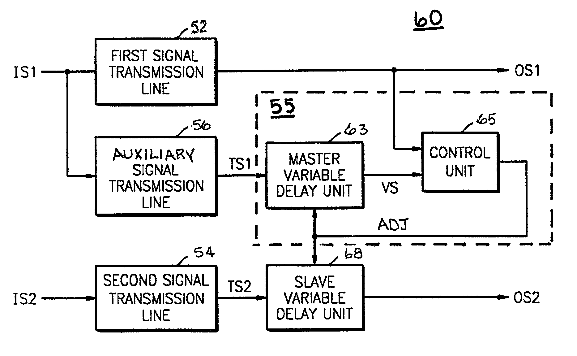
[0031]Referring now to FIG. 5, a general embodiment according to the invention is described. A signal transmission circuit 50 includes first and second signal transmission paths 52 and 54. These may be made in any way known in the art, such as in the ways shown in FIG. 3A through FIG. 3E.

[0032]Signal transmission paths 52 and 54 receive input signals IS1, IS2. First signal transmission path 52 outputs a corresponding output signal OS1, with a first delay W1. Second signal transmission path 54 outputs a corresponding temporary signal TS2, with a second delay W2. It is assumed that the second delay W2 is shorter than the first delay W1. If not, then circuit 50 is configured equivalently in the inverse way.

[0033]Importantly according to the invention, circuit 50 also includes an auxiliary signal transmission path 56. In the preferred embodiment, path 56 is a replica of path 54, although that is not necessary for practicing the inventi...


PUM


Abstract

A signal transmission circuit and a method equalize differential delay characteristics of two signal transmission lines. A controllable delay unit is connected serially to the second line, so as to compensate by adding its internal delay. An auxiliary signal transmission line replicates the second transmission line, while it processes the input signal of the first. A controlling unit compares the output signal of the first transmission line and the of the auxiliary signal transmission line, and adjusts dynamically the internal delay of the controllable delay unit, to attain continuous synchronization. A data latch circuit synchronizes the delays of data paths by having one controllable delay units in each of the data paths.

Description

BACKGROUND OF THE INVENTION[0001]1. Field of the Invention.[0002]The present invention relates to an electrical circuit, and more particularly, to a signal transmission circuit and a method for equalizing disparate delay times of signal transmission paths having different delay characteristics, and a data latch circuit of a semiconductor device implementing the same.[0003]2. Description of the Related Art.[0004]When a signal is transmitted via a signal transmission path, it experiences a delay. The time of the delay depends on the individual characteristics and structure of the signal transmission path. Since the resistance and capacitance of the signal transmission path vary, the delay time varies. However, in a circuit such as a data latch circuit for latching data, at the point in time synchronized with a clock signal, it is necessary for two signals or more signals to be input at the same point in time. Thus, it is necessary for the delay times of signal transmission paths havin...

Claims


Application Information

Patent Timeline
IPC IPC(8): H04L7/00H03K3/02H03K5/06H03K5/131H03K5/14H03L7/00H04L1/22H04L25/14
CPCH04L25/14H04L1/22H03K5/06
Inventor LEE, JUNG-BAEKIM, KYU-HYOUN
Owner SAMSUNG ELECTRONICS CO LTD
Why Eureka
Try Eureka