Surface discharge type plasma display panel having an isosceles delta array type pixel

a plasma display panel and surface discharge technology, applied in the direction of radiofrequency control devices, instruments, and address electrodes, can solve the problem of small writing voltage margin, achieve the effect of increasing the whole voltage margin, increasing the writing voltage margin, and easy causing a writing discharg

Inactive Publication Date: 2006-08-08
MITSUBISHI ELECTRIC CORP
View PDF8 Cites 18 Cited by
  • Summary
  • Abstract
  • Description
  • Claims
  • Application Information

AI Technical Summary

Benefits of technology

[0010]The present invention is intended to solve the above problem, and it is a main object of the present invention to increase a writing voltage margin and suppress generation of wrong writing discharge in pair subpixels of an AC surface discharge type PDP having an isosceles delta array type pixel.
[0027]According to the eight aspect of the present invention, also in the isolated subpixel region, it is possible to suppress deviation of the center of luminescence intensity distribution from the position of the vertical direction central axis of this region and this makes it more easily to achieve a color separation improvement effect.

Problems solved by technology

There arises a new problem in an AC surface discharge type PDP having isosceles delta array type pixels, however, that a writing voltage margin is small.

Method used


Image

  • Surface discharge type plasma display panel having an isosceles delta array type pixel
  • Surface discharge type plasma display panel having an isosceles delta array type pixel
  • Surface discharge type plasma display panel having an isosceles delta array type pixel

Examples


Embodiment Construction

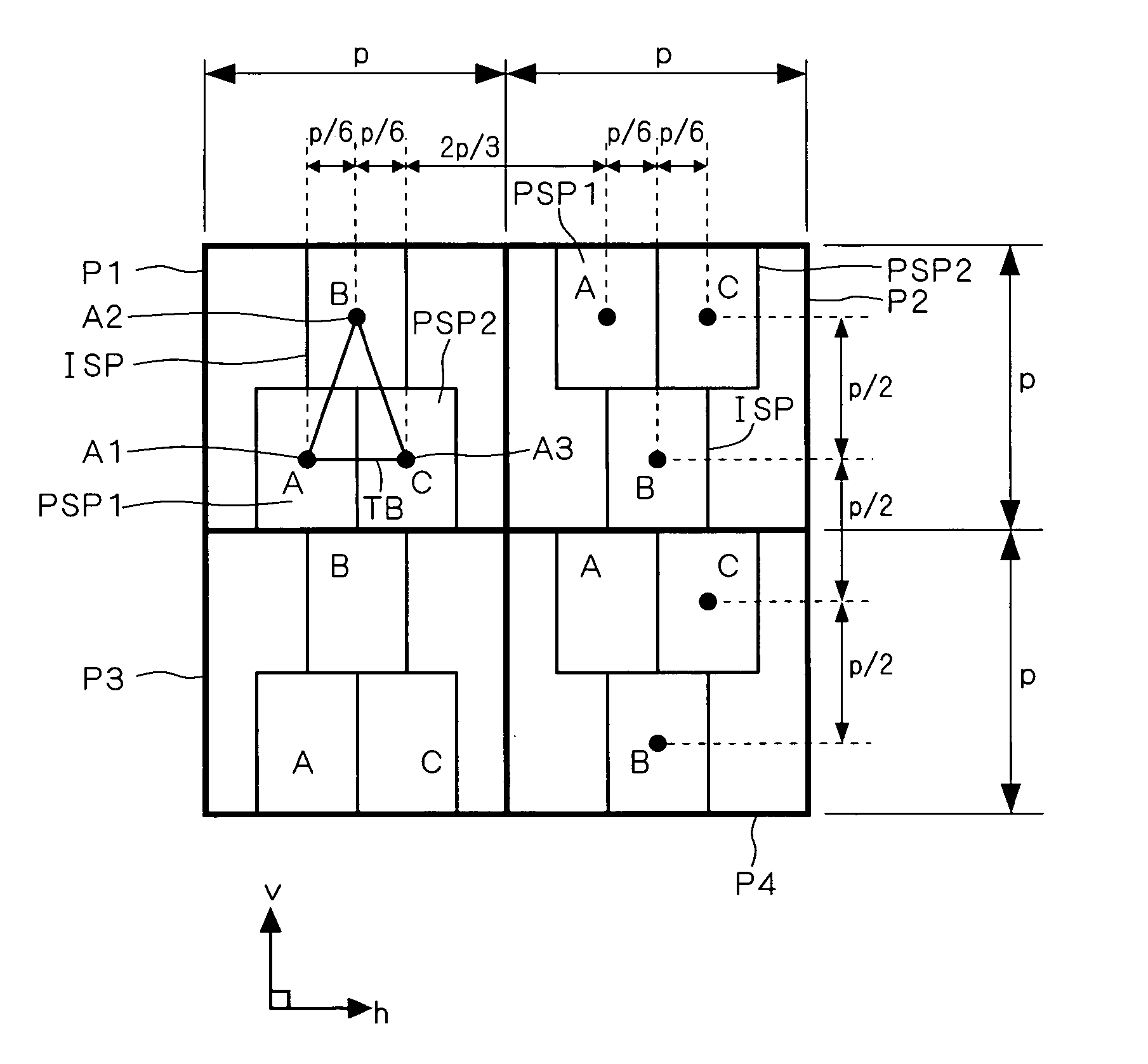
[0042]Since an AC drive surface discharge reflection type PDP in accordance with the present invention has an isosceles delta array type pixel, now, discussion will be made first on a structure of the isosceles delta array type pixel and definition of respective subpixels, referring to figures.

[0043]FIG. 1 is a view schematically showing the structure of the isosceles delta array type pixel. FIG. 1 shows four isosceles delta array type pixels P1, P2, P3 and P4 which are adjacent to one another. The pixels P1 and P3 which are adjacent to each other in a vertical direction (a second direction) v have the same subpixel array structure, and similarly the pixels P2 and P4 have the same subpixel array structure. Herein, taking the pixel P1 as an example, the structure of the pixels P1, P2, P3 and P4 will be described.

[0044]As shown in FIG. 1, a pixel P1 represented as a square having a pitch p is constituted of three subpixels PSP1, PSP2 and ISP, and center points of these subpixels PSP1,...


PUM


Abstract

The present invention relates to an AC drive surface discharge type plasma display panel having an isosceles delta array type pixel. The background art has a problem of being apt to cause a wrong writing discharge and having a narrow writing voltage margin. Then, in the present invention, transparent electrodes for X electrode (T3, T4) in first and second pair subpixel regions (PSPR1, PSPR2) of an isosceles delta array type pixel (P1) are provided at portions farther away from a first write electrode (Wj(B)) in an isolated subpixel region (ISPR). Specifically, a central axis of the third transparent electrode (T3) along a vertical direction (v) is positioned closer to an extending portion (WAE) of a second write electrode (Wj(A)) from a vertical direction central axis of the first pair subpixel region (PSPR1). Similarly, a vertical direction central axis of the fourth transparent electrode (T4) is positioned closer to an extending portion (WCE) of a third write electrode (Wj(C)) from a vertical direction central axis of the second pair subpixel region (PSPR2). The present invention is mainly used for a display device such as a plasma television.

Description

TECHNICAL FIELD[0001]The present invention relates to a surface discharge type plasma display panel (hereinafter, a plasma display panel is also referred to simply as a “PDP”) having an isosceles delta array type pixel constituted of three subpixels (also referred to simply as “cells”) disposed at the respective vertices of an isosceles triangle, and more particularly to a technique to improve driving characteristic of the PDP.BACKGROUND ART[0002]A delta array type pixel is one pixel constituted of three subpixels arranged at vertices of a triangle, and an exemplary case where such-a delta array type pixel is applied to an AC surface discharge type PDP is disclosed in Japanese Patent Application Laid Open Gazette No. 2000-357463.[0003]Further, a method of reducing a circuit cost by commonality of two data electrodes which is based on this structure (this method is referred to as “W electrode common address driving method”) is disclosed in Japanese Patent Application Laid Open Gazett...

Claims


Application Information

Patent Timeline
Patent Type & Authority Patents(United States)
IPC IPC(8): G09G3/28H01J11/12H01J11/22H01J11/24H01J11/26H01J11/32H01J11/34H01J11/36
CPCH01J11/12H01J11/32H01J11/36H01J2211/365H01J2211/323H01J2211/326H01J11/22H01J11/24H01J11/26
Inventor HARADA, SHIGEKISANO, KOUYURA, SHINSUKE
Owner MITSUBISHI ELECTRIC CORP
Why Eureka
Try Eureka