Discharge methods and systems in electrophotography

a technology of electrophotography and discharge method, applied in the field of electrophotography, can solve the problems of large power supply space, large area of machine space occupied by corona devices, contamination and other problems

Inactive Publication Date: 2006-08-15
SAMSUNG ELECTRONICS CO LTD
View PDF23 Cites 6 Cited by
  • Summary
  • Abstract
  • Description
  • Claims
  • Application Information

AI Technical Summary

Benefits of technology

[0017]In an electrophotographic imaging system or any other electrostatic imaging system where images are formed by charging a surface, imagewise discharging the surface and applying toner to the surface to form a latent, intermediate or final image, and then the surface is recharged to provide additional imaging capability, a non-contact grounding system is used. A conductive edge on a photoconductive element used in the imaging process is ionically charged to control the level of charge on the element, preferably to alter the charge on the conductive element to the charge level desired before the recharging is effected. The ionic charging is preferably provided by a separate corona-type charging element that follows the sequence (and location) of the primary charging system and the toner station. A conductive strip is preferably provided on an edge of the photoconductive element so that a small secondary corona-type charging device may be positioned to overlay the conductive strip. By charging the strip, the charge on the photoconductor may be balanced or neutralized.

Problems solved by technology

A common problem in contemporary charging units is that toner supplied from the developing unit often sticks on an unexposed area of the photosensitive drum in the vicinity of the edges of the recording medium, so that contamination occurs.
Heretofore, these corona devices required large power supplies to meet high current and voltage requirements, were costly and took up a large area of machine space.
This was thought to be impossible because conventional thinking on corona generators and experience had taught that reducing the cavity partly surrounding the corotron and bringing the corotron closer to a receiver surface would cause arcing to occur and burn out the wire corotron and damage the photoreceptor.
Also, it was thought that the use of long thin wires (0.0015″) and small radius cavities would cause singing and sagging in the wires.
Since the conductive layer is frequently a thin vapor deposited metal, long life cannot be achieved with an ordinary electrical contact that rubs directly against the thin conductive layer.
However, such an arrangement is generally not suitable for extended runs in copiers, duplicators and printers.
However, such a relatively thick grounding strip layer is still subject to erosion which contributes to the formation of undesirable “dirt” in high volume imaging devices.
Erosion is particularly severe in electrographic imaging systems utilizing metallic grounding brushes or sliding metal contacts.
Also described in systems utilizing a timing light in combination with a timing aperture in the grounding strip layer for controlling various functions of imaging devices is the erosion of the grounding strip layer by devices such as stainless steel grounding brushes and sliding metal contacts is frequently so severe that the grounding strip layer is worn away and becomes transparent thereby allowing light to pass through the grounding strip layer and creating false timing signals which in turn can cause the imaging device to prematurely shut down.
Moreover, the opaque conductive particles formed during erosion of the grounding strip layer tends to drift and settle on other components of the machine such as the lens system, corotron, other electrical components, and the like to adversely affect machine performance.
Also, due to the rapid erosion of the grounding strip layer, the electrical conductivity of the grounding strip layer can decline to unacceptable levels during extended cycling.

Method used


Image

  • Discharge methods and systems in electrophotography
  • Discharge methods and systems in electrophotography
  • Discharge methods and systems in electrophotography

Examples


Embodiment Construction

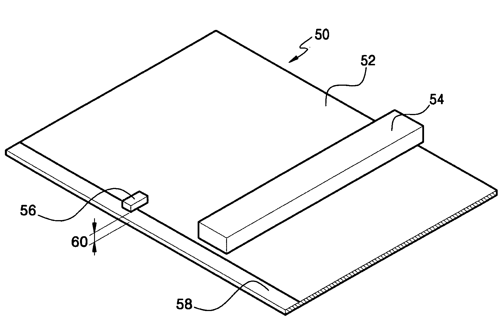
[0022]An important consideration to remember in the field of electrophotography is the fact that it is necessary to electrostatically clean the surface on which the latent charge image is formed in between imaging process steps. If the surface is not cleaned and evenly recharged, spurious charging, and hence spurious imaging, will remain on that surface. It is not necessarily sufficient to merely recharge the surface with the primary corona device, as the remaining charge distribution will leave a background latent image of charge, to which would be added a uniform additive amount of ionic charging. This would be insufficient quality for most commercial uses. It is therefore at least desirable to clean the static charging on the surface (bringing the charge to a uniform distribution as close to zero as possible) before the primary corona charging system adds the overall uniform charge to the photoconductor surface.

[0023]A method may be performed to provide latent charge images on a ...


PUM

PropertyMeasurementUnit
voltagesaaaaaaaaaa
voltagesaaaaaaaaaa
areaaaaaaaaaaa

Abstract

Latent charge images are provided on a photoconductor element having a photoconductive layer with a conductive stripe. This process is performed by charging the photoconductive layer with a charge having a particular vector to form a uniform charge on the photoconductive layer; and subsequently charging the conductive stripe with a charge having a vector that is opposite the vector of the charge on the photoconductive layer to lower the charge content in the photoconductive layer. The first charge may be provided by a first corona charging device and the subsequent charge may be applied by a second corona discharge device focused on a conductive stripe.

Description

BACKGROUND OF THE INVENTION[0001]1. Field of the Invention[0002]The present invention relates to the field of electrophotography, particularly electrophotography methods and apparatus. More particularly the present invention relates to the field of imaging with electrophotographic processes wherein photoconductive substrates are charged, imagewise discharged, toned, imaged (e.g., with fusion or transfer) and recharged, usually with an intermediate charge cleaning or discharge step (intermediate of the imaging and recharge step) that is typically an electromechanical connection[0003]2. Background of the Art[0004]An electrophotographic printing apparatus such as a copy machine or a printer produces electrostatic latent images on a photosensitive drum by converting digital signals corresponding to image data generated from a computer or a copy of an original document into light signals. The signals are sent through an exposure device, and then printed by fixing a toner on paper. A deve...

Claims


Application Information

Patent Timeline
Patent Type & Authority Patents(United States)
IPC IPC(8): G03G15/02G03G21/00G03G15/045G03G21/06
CPCG03G15/0208G03G15/0291G03G2215/026B24B3/44B24B3/54B24B23/08
Inventor BRENNER, ROBERT E.
Owner SAMSUNG ELECTRONICS CO LTD
Why Eureka
Try Eureka