Semiconductor device with wiring layers forming a capacitor

a technology of metal insulating film and capacitor, which is applied in the direction of fixed capacitor details, stacked capacitors, fixed capacitors, etc., can solve the problems of reducing complicating the manufacturing process of semiconductor devices, so as to improve the capacitance value of capacitors, stabilize the operation of semiconductor devices, and improve the effect of capacitors

Active Publication Date: 2006-08-22
RENESAS ELECTRONICS CORP
View PDF9 Cites 6 Cited by
  • Summary
  • Abstract
  • Description
  • Claims
  • Application Information

AI Technical Summary

Benefits of technology

[0022]Furthermore, the semiconductor device according to the present invention comprises an integrated circuit section, and the diameter of the first and second via may be larger than the diameter of the via provided in the integrated circuit section. Thus, the side area of the first and second via is increased, the gap between the first via and the second via becomes small, and the capacitance value between the first and second via is increased.
[0023]Still further, the first terminal is connected to ground wiring, the second terminal is connected to power source wiring, and the capacitor may be a decoupling capacitor connected to a power source in parallel. Thus, power source noise can be absorbed, and the operation of the semiconductor device is stabilized.
[0024]Further, the semiconductor device according to the present invention comprises an upper electrode, which is provided in a region including a region immediately under the first and second electrodes and connected to one of the first and second terminals, an insulating film provided under the upper electrode, and a lower electrode, which is provided under the insulating film and connected to the other one of the first and second terminals, and another capacitor may be formed between the upper electrode and the lower electrode. Thus, a total capacitance value of the capacitors and another capacitor can be obtained, which further improves the capacitance value of capacitor per unit area.
[0025]Furthermore, the semiconductor device comprises an N-type semiconductor layer, which is provided in a region including the region immediately under the first and second electrodes and connected to one terminal out of the first and second terminals, to which higher potential is applied, and a P-type semiconductor layer, which is provided in a region including the region immediately under the electrodes so as to contact the N-type semiconductor layer and connected to one terminal out of the first and second terminals, to which lower potential is applied, and still another capacitor may be formed between the N-type semiconductor layer and the P-type semiconductor layer. Thus, a total capacitance value of the capacitor and still another capacitor can be obtained, which further improves the capacitance value of capacitor per unit area.
[0026]Further, the semiconductor device comprises a semiconductor substrate arranged under the wiring layers, and the semiconductor substrate includes an N-type semiconductor region, which is provided in a region including the region immediately under the first and second electrodes and connected to one terminal out of the first and second terminals, to which higher potential is applied, and a P-type semiconductor region, which is provided in a region including the region immediately under the electrodes so as to contact the N-type semiconductor region and connected to one terminal out of the first and second terminals, to which lower potential is applied, and still another capacitor may be formed between the N-type semiconductor region and the P-type semiconductor region. Thus, a total capacitance value of the capacitor and still another capacitor can be obtained, which further improves the capacitance value of capacitor per unit area.
[0027]According to the present invention, the first and second electrodes can be formed simultaneously with the regular wiring and the first and second via can be formed simultaneously with the regular via in each wiring layer of the semiconductor device. For this reason, the semiconductor device equipped with the MIM capacitor can be fabricated without the need of the special process for forming the capacitors.

Problems solved by technology

However, the above-described prior art has the following problems.
However, when a regular interlayer insulating film is used as the capacitance insulating film, the capacitance insulating film becomes too thick because the thickness of the interlayer insulating film is approximately 0.3 to 1.0 μm, and the capacitance value of capacitor is reduced.
Consequently, the manufacturing process of semiconductor device becomes complicate, which leads to an increased manufacturing cost.

Method used


Image

  • Semiconductor device with wiring layers forming a capacitor
  • Semiconductor device with wiring layers forming a capacitor
  • Semiconductor device with wiring layers forming a capacitor

Examples


Embodiment Construction

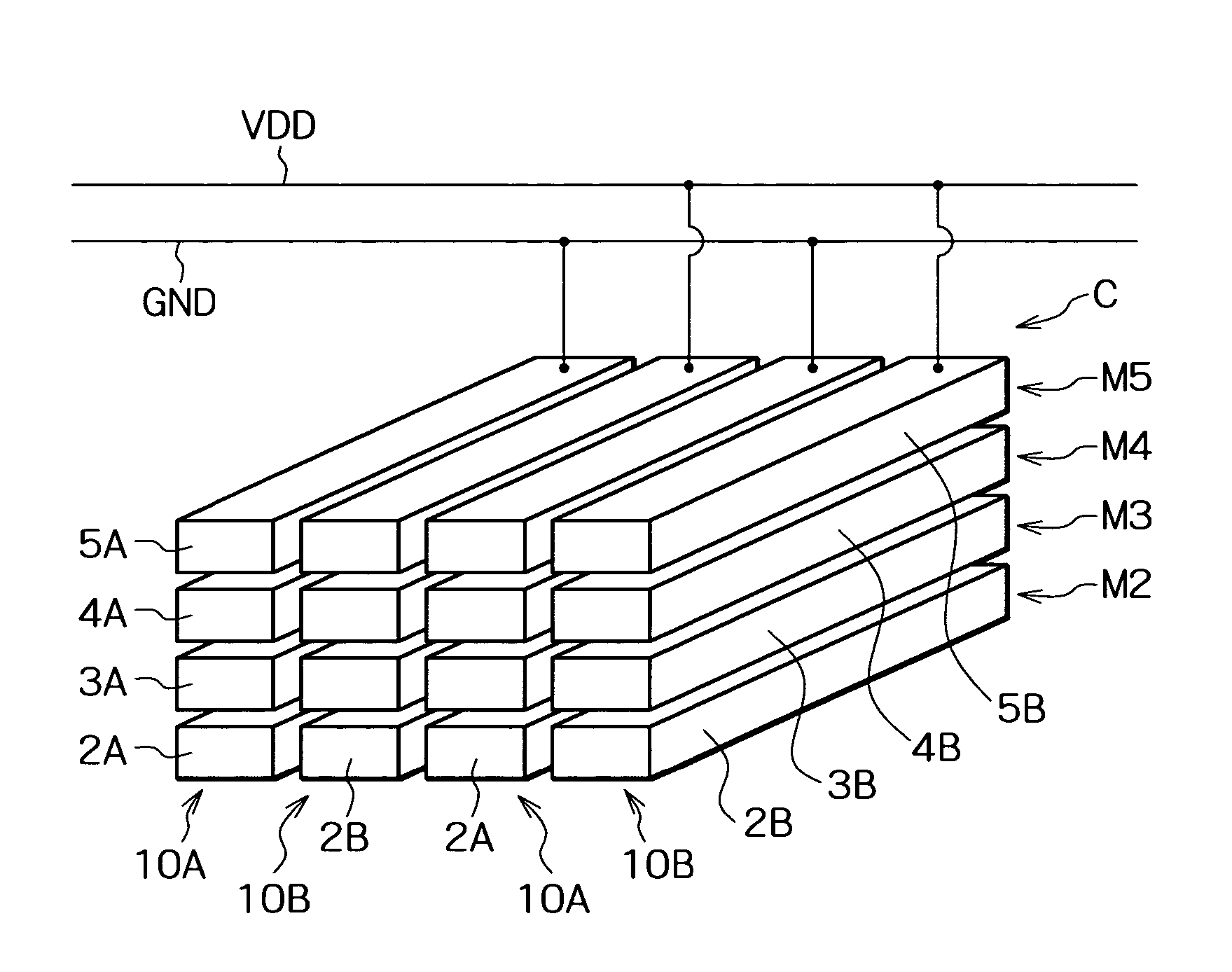
[0033]A preferred embodiment of the present invention will be specifically described as follows referring to the attached drawings. FIG. 3 is the perspective view showing the MIM capacitor provided in the semiconductor device according to this embodiment, FIG. 4 is the plan view showing the MIM capacitor, FIG. 5A is the sectional view by A—A line shown in FIG. 4, and FIG. 5B is the sectional view by B—B line.

[0034]As shown in FIG. 3, the semiconductor device according to this embodiment is provided with a semiconductor substrate (not shown), and a plurality of wiring layers, nine layers for example, are laminated on the semiconductor substrate. Out of the nine wiring layers, the second to fifth wiring layers (hereinafter, referred to as wiring layers M2 to M5) from the bottom, that is, from the semiconductor substrate are middle wiring layers, which are provided using the same design rule with each other. The sixth to ninth wiring layers (hereinafter, referred to as wiring layers M6...


PUM


Abstract

A semiconductor device, in which four pieces of strip-shaped electrodes, whose longitudinal directions are the same, are formed in each layer of a plurality of wiring layers that are provided by a same design rule with each other, simultaneously with regular wirings. In each wiring layer, two pieces each of first electrode and second electrode are formed parallelly with each other, alternately, and remote from each other. Then, the first electrodes formed in each layer are connected to each other by a first via, the second electrodes formed in each layer are connected to each other by a second via, a first structure body formed by connecting the first electrodes and the first via to each other is connected to a ground wiring, and a second structure body formed by connecting the second electrodes and the second via to each other is connected to a power source wiring.

Description

BACKGROUND OF THE INVENTION[0001]1. Field of the Invention[0002]The present invention relates to a semiconductor device equipped with an MIM (Metal-Insulator-Metal) capacitor, particularly to a semiconductor device whose manufacturing process has been simplified.[0003]2. Description of the Related Art[0004]For example, as disclosed in the literature M. Armacost, et. al. “A High Reliability Metal Insulator Metal Capacitor for 0.18 μm Copper Technology” IEDM2000 pp. 157–160′, a lower electrode, a capacitance insulating film, and an upper electrode are laminated on a substrate in this order to form the MIM capacitor when forming a capacitor in the semiconductor device conventionally.[0005]FIG. 1 is a sectional view showing a semiconductor device equipped with a conventional MIM capacitor. As shown in FIG. 1, in the conventional semiconductor device, an oxide film 102 is provided on a substrate 101, and a lower electrode 103 made of metal is provided thereon. Then, a capacitance insulat...

Claims


Application Information

Patent Timeline
Patent Type & Authority Patents(United States)
IPC IPC(8): H01L27/108H01G4/228H01G4/30H01L29/76H01L29/94H01L21/02H01L23/522H01L27/08
CPCH01L23/5222H01L27/0805H01L28/82H01L2924/3011H01L2924/0002H01L2924/00
Inventor FURUMIYA, MASAYUKIOHKUBO, HIROAKINAKASHIBA, YASUTAKA
Owner RENESAS ELECTRONICS CORP
Why Eureka
Try Eureka