Semiconductor device and manufacturing method thereof

a semiconductor and manufacturing method technology, applied in semiconductor devices, diodes, electrical devices, etc., can solve the problems of increasing cost, reducing the dimensional reduction, and complicated process, and achieves excellent capability, low leakage current, and high capacitance

Active Publication Date: 2009-02-26
GK BRIDGE 1
View PDF4 Cites 0 Cited by
  • Summary
  • Abstract
  • Description
  • Claims
  • Application Information

AI Technical Summary

Benefits of technology

[0029]According to this method, the thickness of the second electrode formation film becomes larger than that of the first electrode formation film in step (b). Therefore, when impurities are implanted to each electrode in step (c), the impurities are less likely to reach the interface region with the second insulating film in the second electrode formation film. As a result, the first electrode and the second electrode having different impurity concentration distributions from each other can be obtained in step (d). Therefore, when a voltage is applied to each electrode, t...

Problems solved by technology

Therefore, an additional oxidation step is required to form an insulating film having a different film quality, and impurities that are implanted into an electrode need to be sufficiently controlled in order to ensure reliability of an insulating film...

Method used


Image

  • Semiconductor device and manufacturing method thereof
  • Semiconductor device and manufacturing method thereof
  • Semiconductor device and manufacturing method thereof

Examples


first embodiment

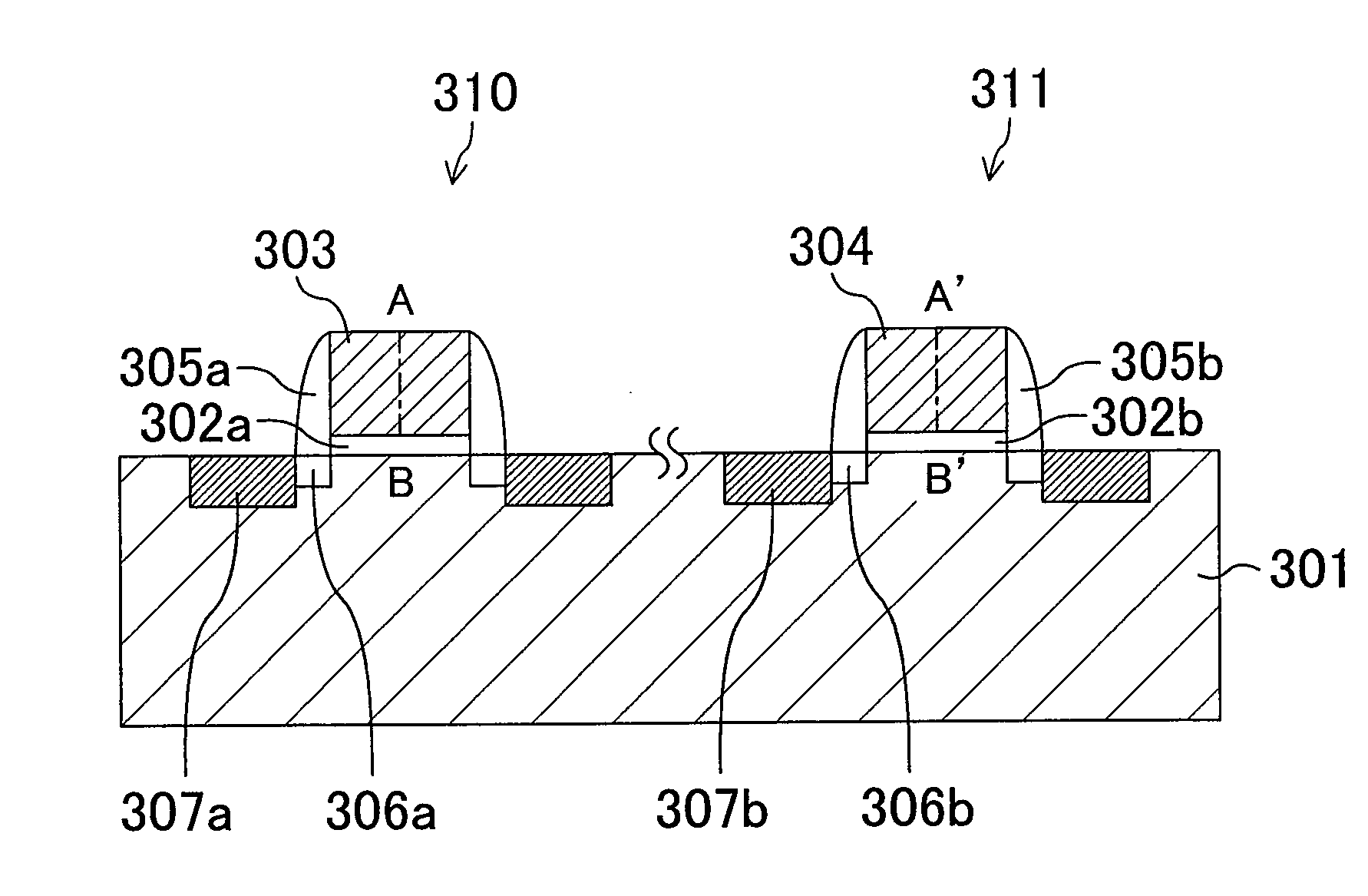
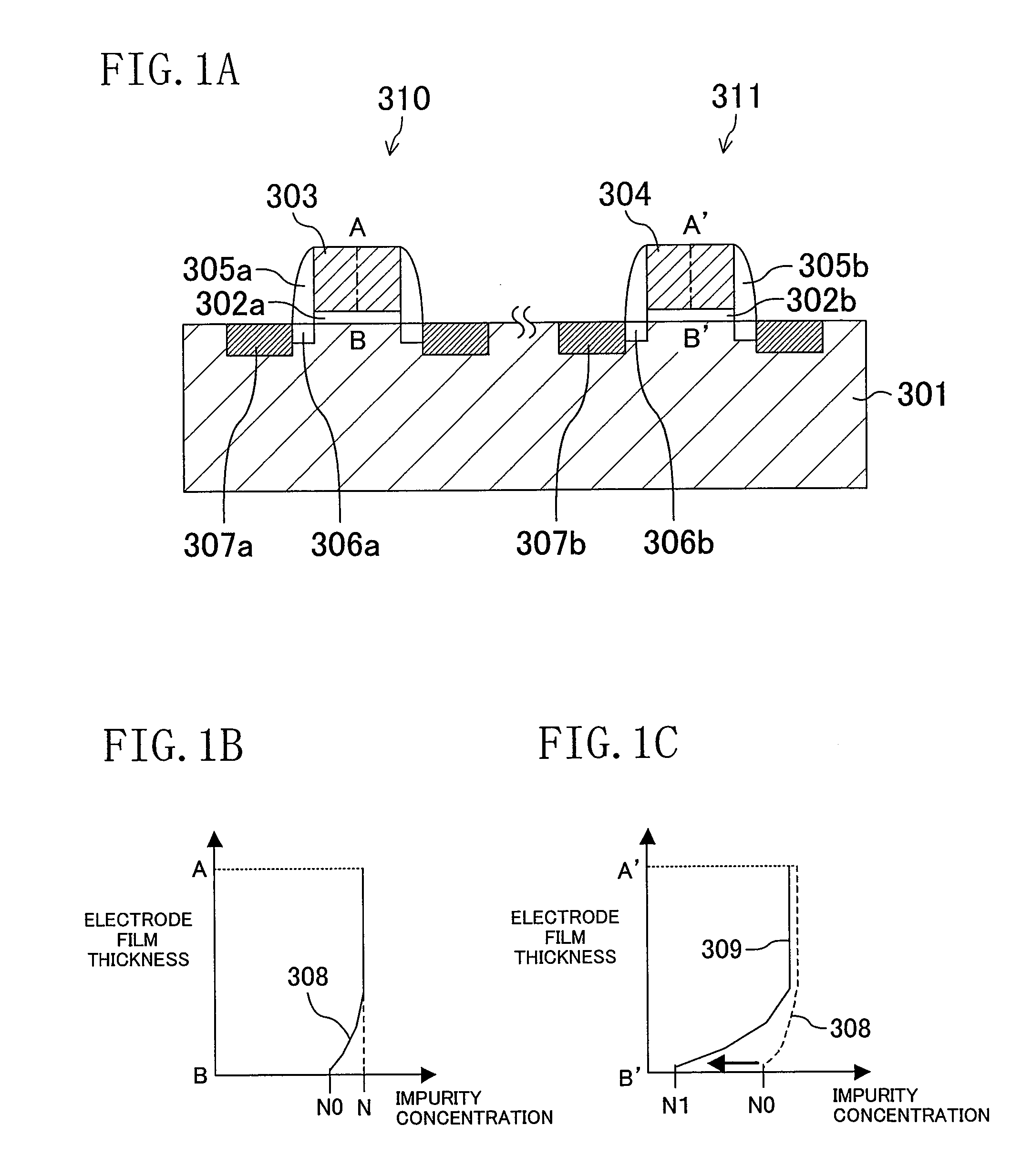
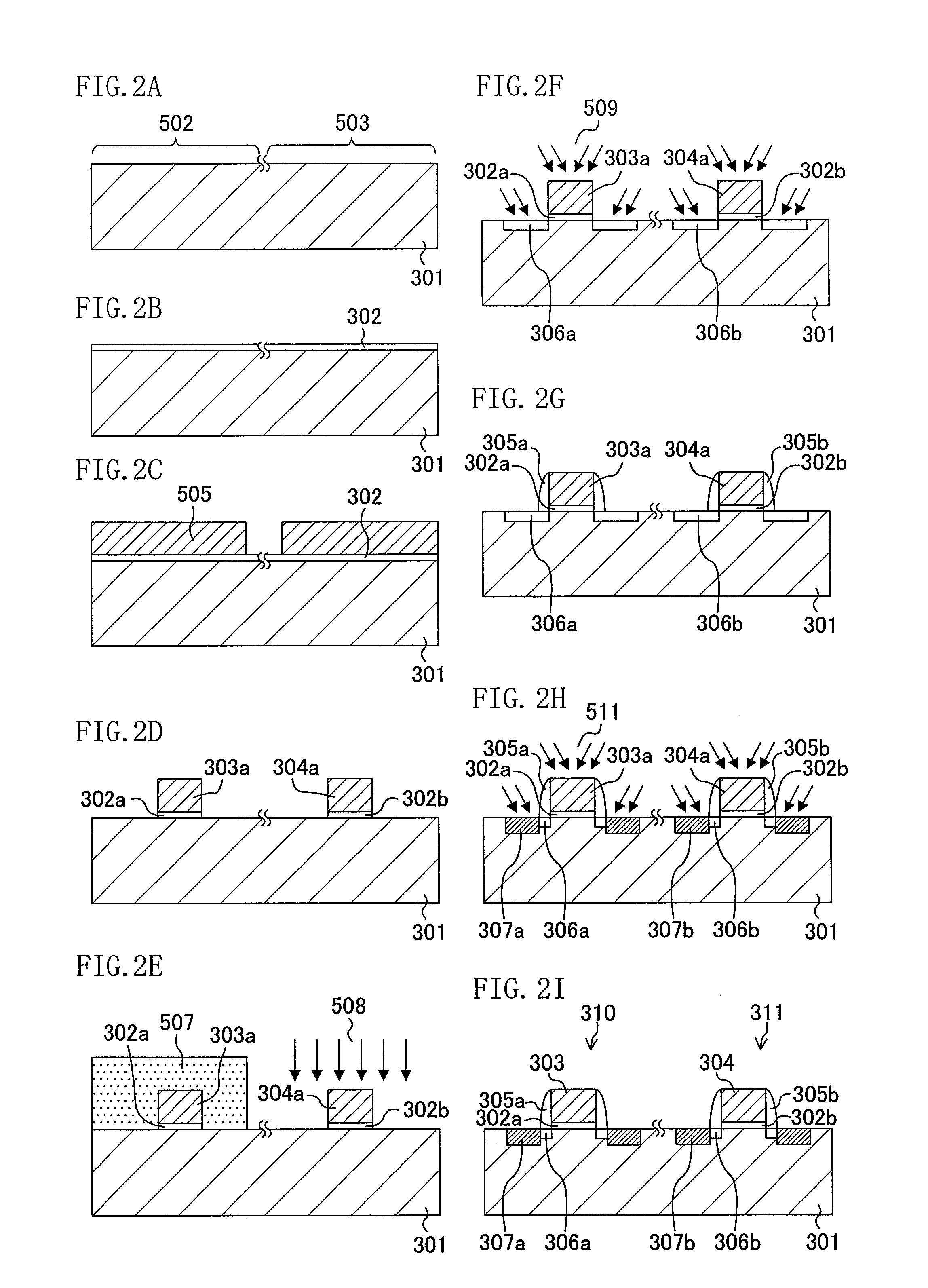
[0040]Hereinafter, a semiconductor device and a manufacturing method thereof according to a first embodiment of the invention will be described with reference to the figures. FIG. 1A shows a structure of the semiconductor device according to this embodiment.

[0041]As shown in FIG. 1A, the semiconductor device of this embodiment includes a semiconductor substrate 301, and a first MOS type capacitor 310 and a second MOS type capacitor 311 that are formed on the semiconductor substrate 301. The first MOS type capacitor 310 includes a first insulating film 302a formed on the semiconductor substrate 301, a first electrode 303 formed on the first insulating film 302a, a sidewall 305a formed on the respective side surfaces of the first insulating film 302a and the first electrode 303, and an impurity region 306a and a high concentration impurity region 307a that are formed in the semiconductor substrate 301. The impurity region 306a and the high concentration impurity region 307a are respec...

second embodiment

[0057]Hereinafter, a semiconductor device and a manufacturing method thereof according to a second embodiment of the invention will be described with reference to the figures. FIG. 4A shows a structure of the semiconductor device of this embodiment. Note that the structure of the semiconductor device of this embodiment is only partially different from that of the semiconductor device of the first embodiment. Therefore, the same portions will be described briefly.

[0058]As shown in FIG. 4A, the semiconductor device of this embodiment includes a semiconductor substrate 401, and a first MOS type capacitor 420 and a second MOS type capacitor 421 that are formed on the semiconductor substrate 401. The first MOS type capacitor 420 includes a first insulating film 402a, a first electrode 403, a sidewall 405a, an impurity region 406a, and a high concentration impurity region 407a. The first insulating film 402a is formed on the semiconductor substrate 401 and the first electrode 403 is forme...

third embodiment

[0073]Hereinafter, a semiconductor device and a manufacturing method thereof according to a third embodiment of the invention will be described with reference to the figures. FIG. 6A is a cross-sectional view showing a structure of the semiconductor device of this embodiment. As shown in FIG. 6A, the structure of the semiconductor device of this embodiment is the same as that of the semiconductor device of the second embodiment (see FIG. 4A). Therefore, description thereof will be omitted.

[0074]As shown in FIG. 6A, the semiconductor device of this embodiment includes a semiconductor substrate 401, and a first MOS type capacitor 820 and a second MOS type capacitor 821 that are formed on the semiconductor substrate 401. Like the semiconductor device of the second embodiment, the thickness of a first electrode 803 is smaller than that of a second electrode 804 by, for example, T0. Accordingly, as shown in FIGS. 6B and 6C, the first electrode 803 and the second electrode 804 have the sa...


PUM


Abstract

A semiconductor device includes a first MOS type capacitor having a first insulating film and a first electrode that are formed on a semiconductor substrate, and a second MOS type capacitor having a second insulating film and a second electrode that are formed on the semiconductor substrate. The first electrode has a first concentration difference as a difference when an impurity concentration in an interface region with the first insulating film is subtracted from an impurity concentration in a top portion of the first electrode. The second electrode has a second concentration difference as a difference when an impurity concentration in an interface region with the second insulating film is subtracted from an impurity concentration in a top portion of the second electrode. The second concentration difference is larger than the first concentration difference.

Description

BACKGROUND OF THE INVENTION[0001]1. Field of the Invention[0002]The invention relates to a semiconductor device having, for example, a MOS (Metal Oxide Semiconductor) type capacitor and a manufacturing method thereof.[0003]2. Related Art[0004]With recent improvement in integration and functionality of semiconductor integrated circuit devices, higher capacitance and lower leakage current characteristics have been required for MOS type capacitor elements (MOS type capacitors). However, it is difficult to satisfy these two characteristics with the same MOS type capacitor. Therefore, it has been considered to form a capacitor having a high capacitance value (high capacitance capacitor) and a capacitor having a low leakage current value (low leakage current capacitor) depending on the applications in order to implement a MOS type capacitor satisfying the two characteristics. A typical method for forming these two kinds of capacitors is to form a thin insulating film for a high capacitanc...

Claims


Application Information

Patent Timeline
IPC IPC(8): H01L29/94H01L21/20
CPCH01L21/26506H01L27/0808H01L29/94H01L29/6659H01L29/7833H01L27/0811H01L21/2658
Inventor SHIBATA, YOSHIYUKI
Owner GK BRIDGE 1
Why Eureka
Try Eureka