Semiconductor device and method of manufacturing the same

a technology of semiconductors and semiconductors, applied in semiconductors, solid-state devices, capacitors, etc., can solve the problems of degrading the reliability of the device, difficult to form a deep contact hole, and difficult for the device to perform stably, so as to achieve a high degree of freedom and increase the capacity value

Inactive Publication Date: 2007-09-11
RENESAS ELECTRONICS CORP
View PDF3 Cites 0 Cited by
  • Summary
  • Abstract
  • Description
  • Claims
  • Application Information

AI Technical Summary

Benefits of technology

[0016]Accordingly, it is an object of the present invention to provide a semiconductor device wherein a capacitance value can be increased without a compromise in designing a position of a capacitor, and a method of manufacturing such a semiconductor device.
[0018]According to the present invention, the second conductive plug and the third conductive plug for electrically connecting the first conductive plug and an interconnect etc. formed on the third interlayer dielectric film are formed in a “double stack” structure. Such arrangement permits increasing an integration level of the semiconductor device, as well as securing a sufficient height of the capacitor even though it may be difficult to form a deep contact hole. As a result, a desired capacitance value can be maintained.
[0021]According to the present invention, a conductor such as a metal plug is formed in advance in the second interlayer dielectric film, which is where the capacitor is to be formed. Such constitution permits increasing a surface area of a lower electrode of the capacitor, and thus increasing a capacitance value of the capacitor.
[0022]Also, since the conductor such as a metal plug is provided for the purpose of increasing a surface area of the lower electrode, the conductor does not have to be directly connected to the first conductive plug, which eliminates the need to dispose the capacitor right above the first conductive plug. Accordingly, positioning of the capacitor and the first conductive plug is not particularly limited as long as an electric connection, including an indirect connection, can be secured between the capacitor and the first conductive plug. Therefore, higher designing freedom is granted in disposing the capacitor.
[0024]As described above, according to the present invention, a capacitance value can be increased, while securing a high degree of freedom in designing a position of the capacitor.

Problems solved by technology

Therefore, it is difficult to form a deep contact hole when using an ArF stepper.
Further, a decrease in a capacitance value of a memory cell makes it difficult for the device to perform stably, thereby degrading reliability of the device.
Therefore, maintaining the capacitance value of a memory cell at a certain level, despite the increase in integration level, constitutes a key issue.
Therefore, a position where the capacitor contact may be disposed is limited.
Consequently, according to a conventional technique as cited above, a position to form a capacitor is limited, which requires a significant compromise in designing freedom of the semiconductor device.

Method used


Image

  • Semiconductor device and method of manufacturing the same
  • Semiconductor device and method of manufacturing the same
  • Semiconductor device and method of manufacturing the same

Examples


first embodiment

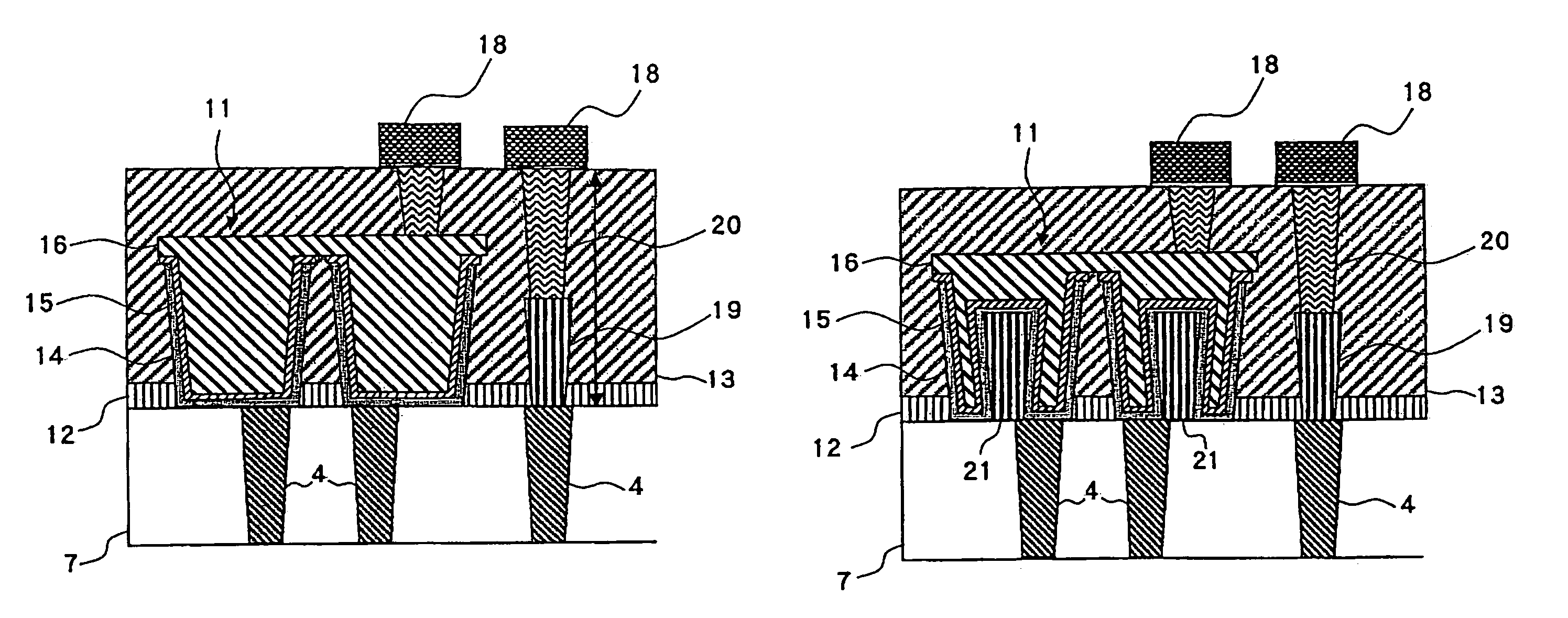
[0038]FIG. 1 is a cross-sectional drawing showing a constitution of a semiconductor device according to a first embodiment of the present invention. In FIG. 1, the same constituent as those in FIG. 11 are given an identical numeral, and description thereof will be omitted. Also, throughout the subsequent passages, a region around the capacitor 11 of FIG. 10 will be referred to, as in the description of FIG. 11.

[0039]In the conventional semiconductor device shown in FIG. 11, the metal interconnect 18 and the capacitor contact 4 are connected via a single contact 17. On the other hand, in a semiconductor device according to this embodiment shown in FIG. 1, two contacts, namely a first contact 19 and a second contact 20, are formed in double stack for connecting the metal interconnect 18 and the capacitor contact 4.

[0040]Forming the first and the second contacts 19, 20 in double stack as in this embodiment permits increasing an integration level of the semiconductor device, as well as ...

second embodiment

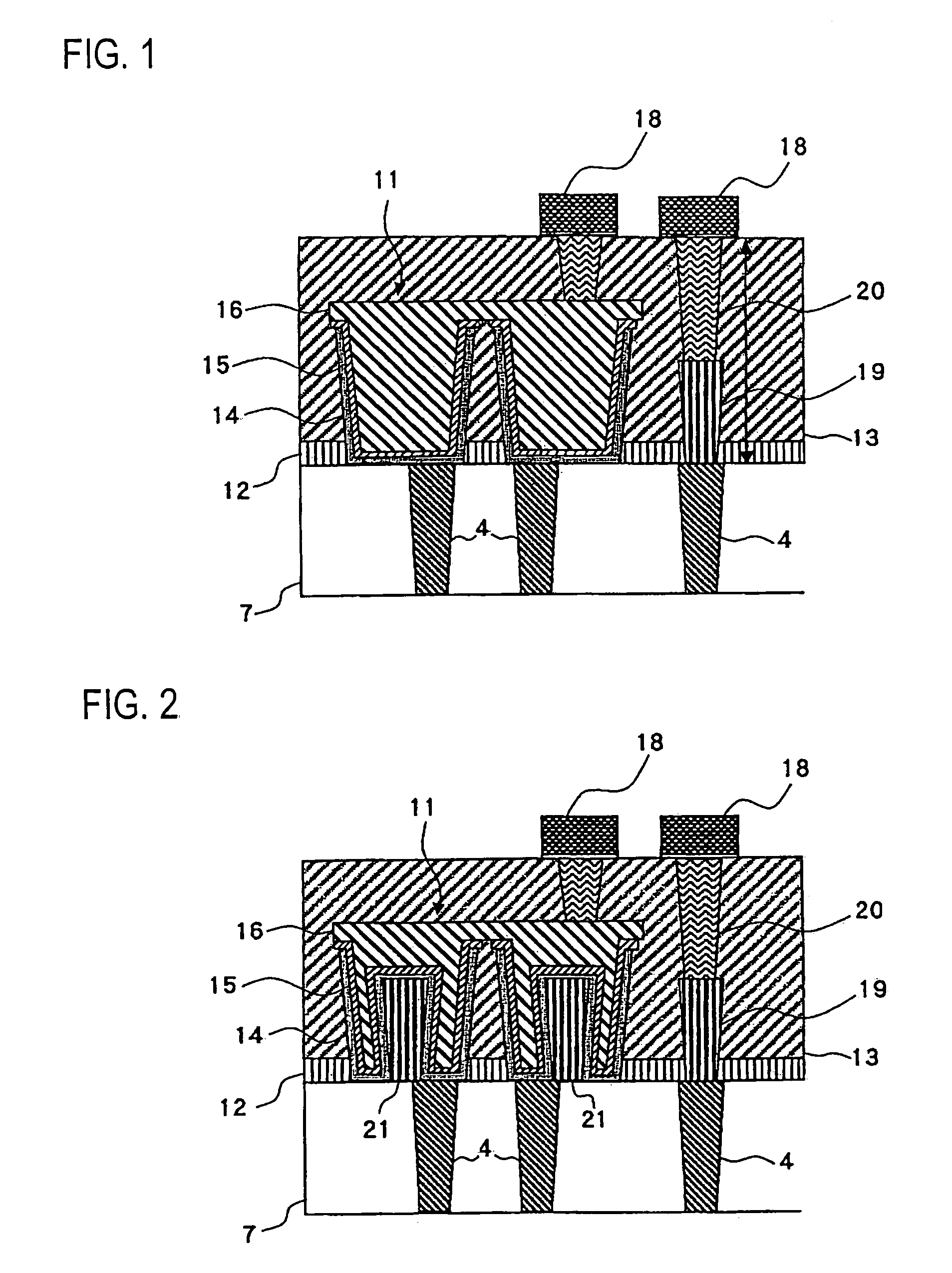
[0043]Now a semiconductor device according to the second embodiment of the present invention will be described.

[0044]FIG. 2 is a cross-sectional drawing showing a constitution of a semiconductor device according to a second embodiment of the present invention. In FIG. 2 also, the same constituent as those in FIG. 1 are given an identical numeral, and description thereof will be omitted.

[0045]The semiconductor device according to this embodiment is different from that of the first embodiment as shown in FIG. 1, in that a tungsten plug 21 is formed in advance in the same step of forming the first contact 19 at a time, in a region of the contact interlayer film 13 where the capacitor 11 is to be located, so as to increase a surface area of the lower electrode 14 of the capacitor 11, and to thus increase a capacitance value. Here, since the tungsten plug 21 is to be formed in the same step as the first contact 19 at a time, the tungsten plug 21 and the first contact 19 are both constitu...


PUM


Abstract

The present invention provides a method of increasing designing freedom of a position to form a capacitor, and increasing a capacitance value thereof. When forming a first contact, a tungsten plug for increasing a surface area of a lower electrode is formed in a contact interlayer film at a region where the capacitor is to be formed. Since the tungsten plug does not have to be formed right above the capacitor contact, a position to form the capacitor is not limited by a position where the capacitor contact is provided.

Description

[0001]This application is based on Japanese patent application No. 2003-324953, the content of which is incorporated hereinto by reference.BACKGROUND OF THE INVENTION[0002]1. Field of the Invention[0003]The present invention is related to a semiconductor device and a method of manufacturing the semiconductor device.[0004]2. Description of the Related Art[0005]A memory cell constituting a DRAM (Dynamic Random Access Memory) generally includes a memory cell transistor and a capacitor. With an object to increase an integration level of the memory cell, a COB (Capacitor Over Bit line) type DRAM in which a capacitor of the DRAM is located in an upper layer of a bit line has been proposed. FIG. 10 shows a constitution of such COB type DRAM.[0006]In this DRAM a MOS transistor formed on a semiconductor substrate, in FIG. 10 a silicon substrate 10, is serving as a memory cell transistor. In an upper layer of the memory cell transistor, a bit line 6 is formed via a cell contact interlayer fil...

Claims


Application Information

Patent Timeline
Patent Type & Authority Patents(United States)
IPC IPC(8): H01L27/108H01L29/76H01L29/94H01L31/119H01L21/768H01L21/02H01L21/8242
CPCH01L27/10811H01L27/10814H01L27/10817H01L27/10852H01L28/91H10B12/312H10B12/318H10B12/315H10B12/033
Inventor INOUE, TOMOKO
Owner RENESAS ELECTRONICS CORP
Why Eureka
Try Eureka