Optical waveguide manufacturing method

Inactive Publication Date: 2006-08-22
PANASONIC CORP
View PDF17 Cites 0 Cited by
  • Summary
  • Abstract
  • Description
  • Claims
  • Application Information

AI Technical Summary

Benefits of technology

[0004]It is an object of the present invention to provide an optical waveguide with a small optical transmission loss. The method for manufacturing an optical waveguide of the present invention is one in which a patterned mask or a resist is placed on the surface of a core layer and then dry etching

Problems solved by technology

A problem encountered with the core layer formed with the above-mentioned multi-component glass is that the optical transmission loss of the optical waveguide tends to be large.
During this proce

Method used


Image

  • Optical waveguide manufacturing method
  • Optical waveguide manufacturing method
  • Optical waveguide manufacturing method

Examples


embodiment 1

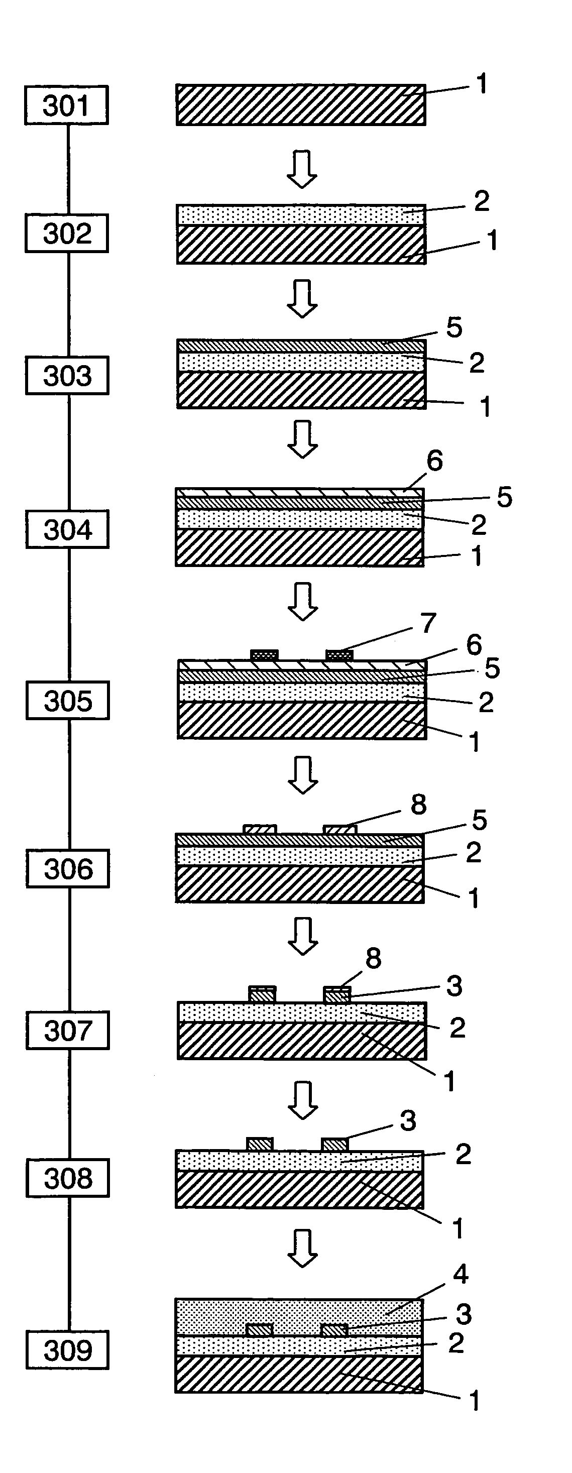
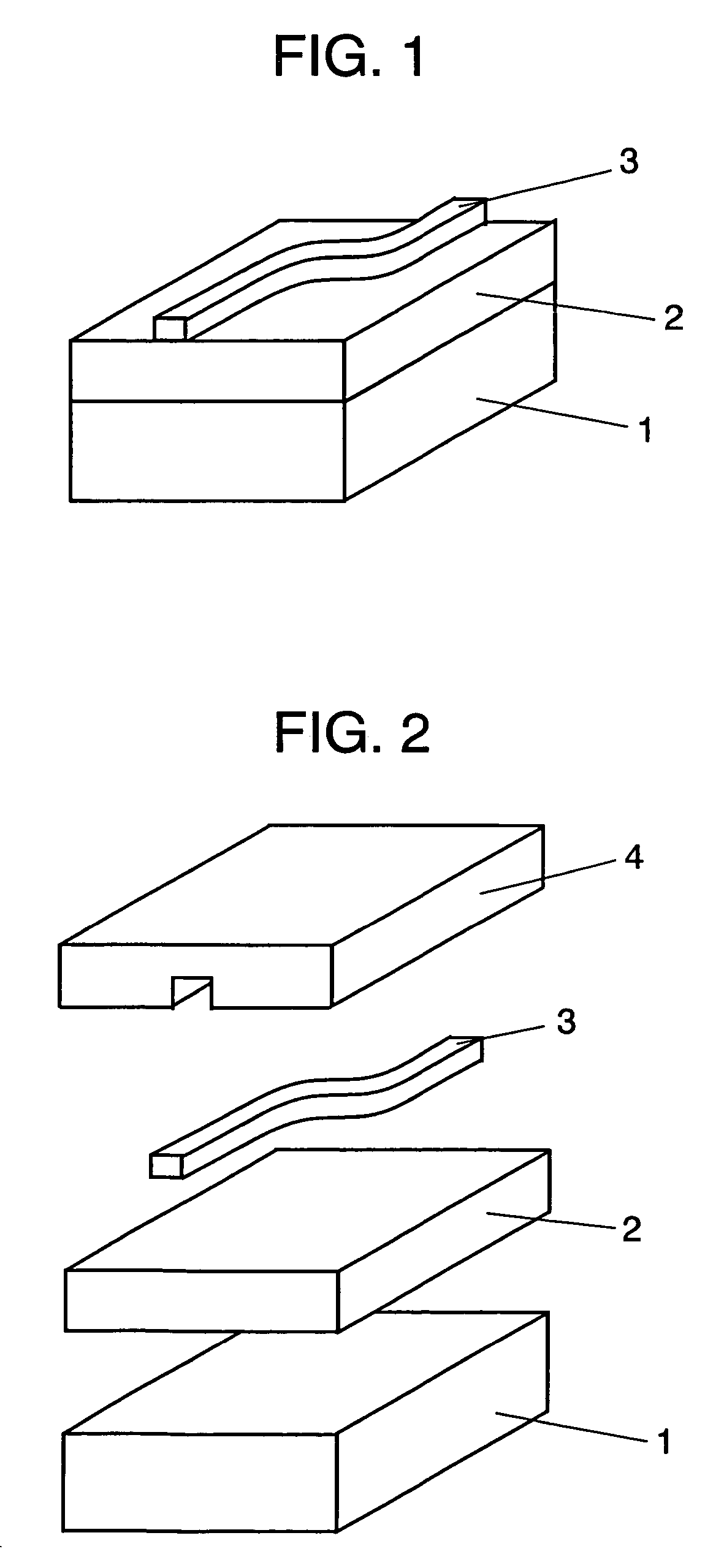
[0015]FIG. 1 is a perspective view to illustrate one of the manufacturing steps of the present invention. Substrate 1 is silicon or various types of glass, for example. Here, various types of glass mean glass that contains at least one of alkaline elements, alkaline earth elements and rare earth elements. First clad layer 2 is formed with SiO2 or various types of glass.

[0016]When the thermal expansion coefficients of substrate 1 and first clad layer 2 are different, thermal stress is sometimes caused. Accordingly, most preferable is that the thermal expansion coefficients of the two are equal, but they can be used when the thermal expansion coefficients are close. Also, when substrate 1 is made of silicon, the first clad may be made by oxidizing silicon into SiO2. Also, substrate 1 and first clad layer 2 may be made of the same material. Core pattern 3 is formed using SiO2 or various types of glass and its refractive index is made slightly greater than that of first clad layer 2.

[00...

embodiment 2

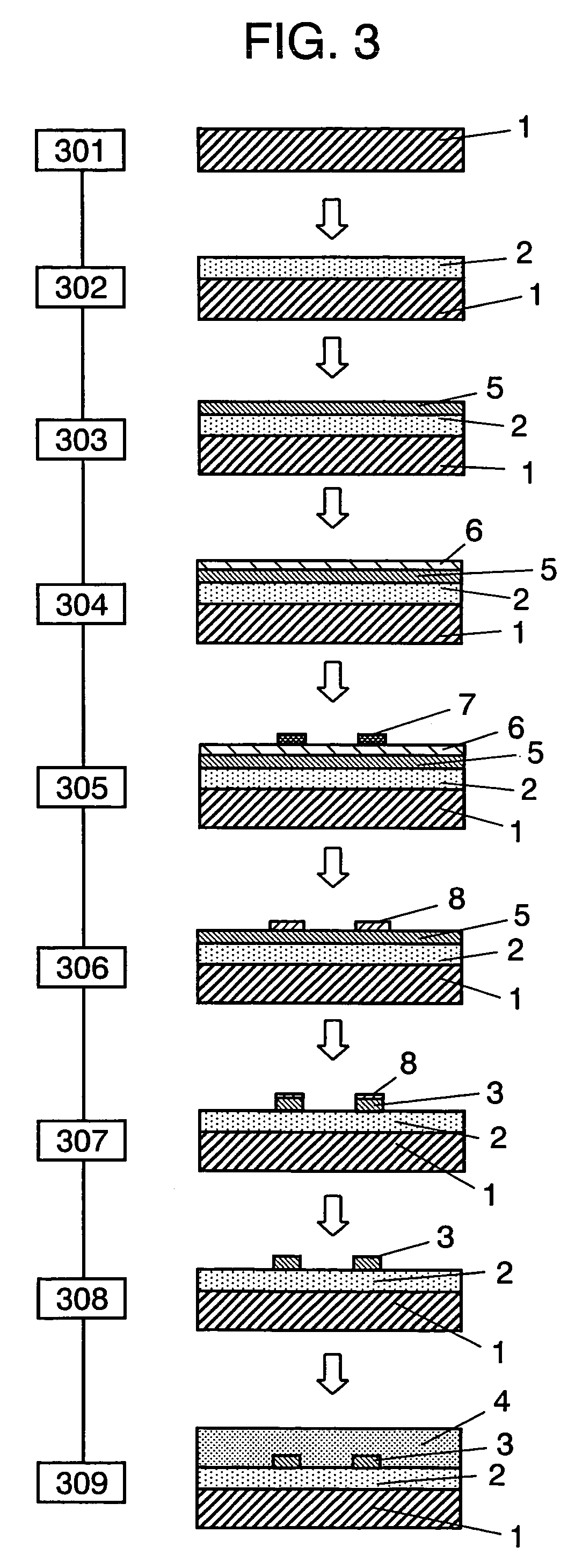
[0038]Referring to FIG. 9, a description of another exemplary embodiment will be given.

[0039]Subsequent to substrate preparation step 901, first clad layer 12 is formed on substrate 11 in first clad formation step 902. In core layer formation step 903, core layer 15 is formed on first clad layer 12, and in subsequent resist processing step 904, resist pattern 17 is provided on the surface of core layer 15. Next, in core etching step 905, core pattern 13 is formed by dry etching core layer 15. After removing resist pattern 17 in resist removal step 906, second clad layer 14 is formed on first clad layer 12 in second clad formation step 907 in a manner such that it covers core pattern 13, thus completing an optical waveguide. In summary, in the embodiment 2, resist pattern 17 itself works as a mask for dry etching.

[0040]In the first and second exemplary embodiments, a description was given of examples of methods for manufacturing an optical waveguide that has a core layer consisting o...


PUM


Abstract

A method for manufacturing an optical waveguide of the present invention is one in which a mask is provided on the surface of a core layer followed by performing dry etching, and the dry etching step includes etching and ashing steps. With this, the irregularities formed on the periphery of a core pattern during manufacture of an optical waveguide can be eliminated, and an optical waveguide with a low optical transmission loss is proved.

Description

TECHNICAL FIELD[0001]The present invention relates to a method for manufacturing optical waveguides having a low optical transmission loss.BACKGROUND ART[0002]As quartz glass based material is used in the core layer of conventional optical waveguides, physical properties of the core layer such as the refractive index and coefficient of thermal expansion are roughly determined by the physical properties of quartz glass. In recent years, there is sometimes a request for changing the physical properties of the core layer. For this reason, proposals have been made to form optical waveguides by using multi-component glass containing such elements as alkaline elements, alkaline earth elements, or rare earth elements. When forming a core layer of an optical waveguide with multi-component glass, physical properties of the glass such as refractive index, thermal expansion coefficient, or glass transition temperature can be freely designed over a wider range by properly changing the glass com...

Claims


Application Information

Patent Timeline
IPC IPC(8): G02B6/10G02B6/12G02B6/136
CPCG02B6/136G02B2006/12176
Inventor TATEHATA, NAOKI
Owner PANASONIC CORP
Why Eureka
Try Eureka