

Method for programming/parallel programming of onboard flash memory by multiple access bus
a technology of onboard flash memory and access bus, which is applied in the direction of information storage, instruments, logic circuits, etc., can solve the problems of low cost, reduced transmission speed which is limited to 9600 bits/s, and physical interface is not suitable for fast data transfer, so as to reduce costs and increase productivity in production lines
- Summary
- Abstract
- Description
- Claims
- Application Information
AI Technical Summary
Benefits of technology
Problems solved by technology
Method used
Image

Examples
Embodiment Construction
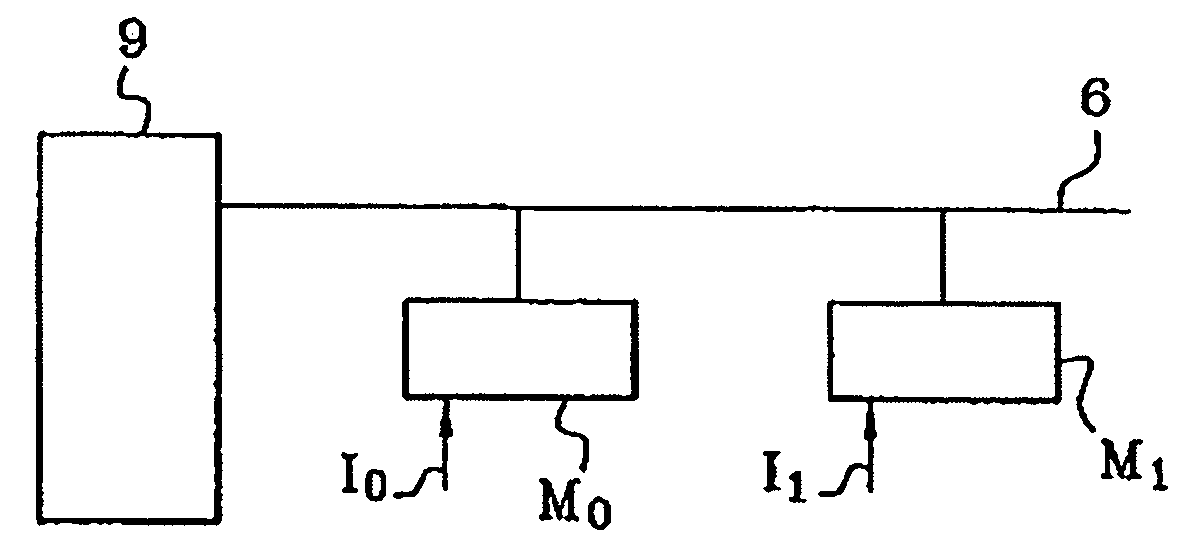
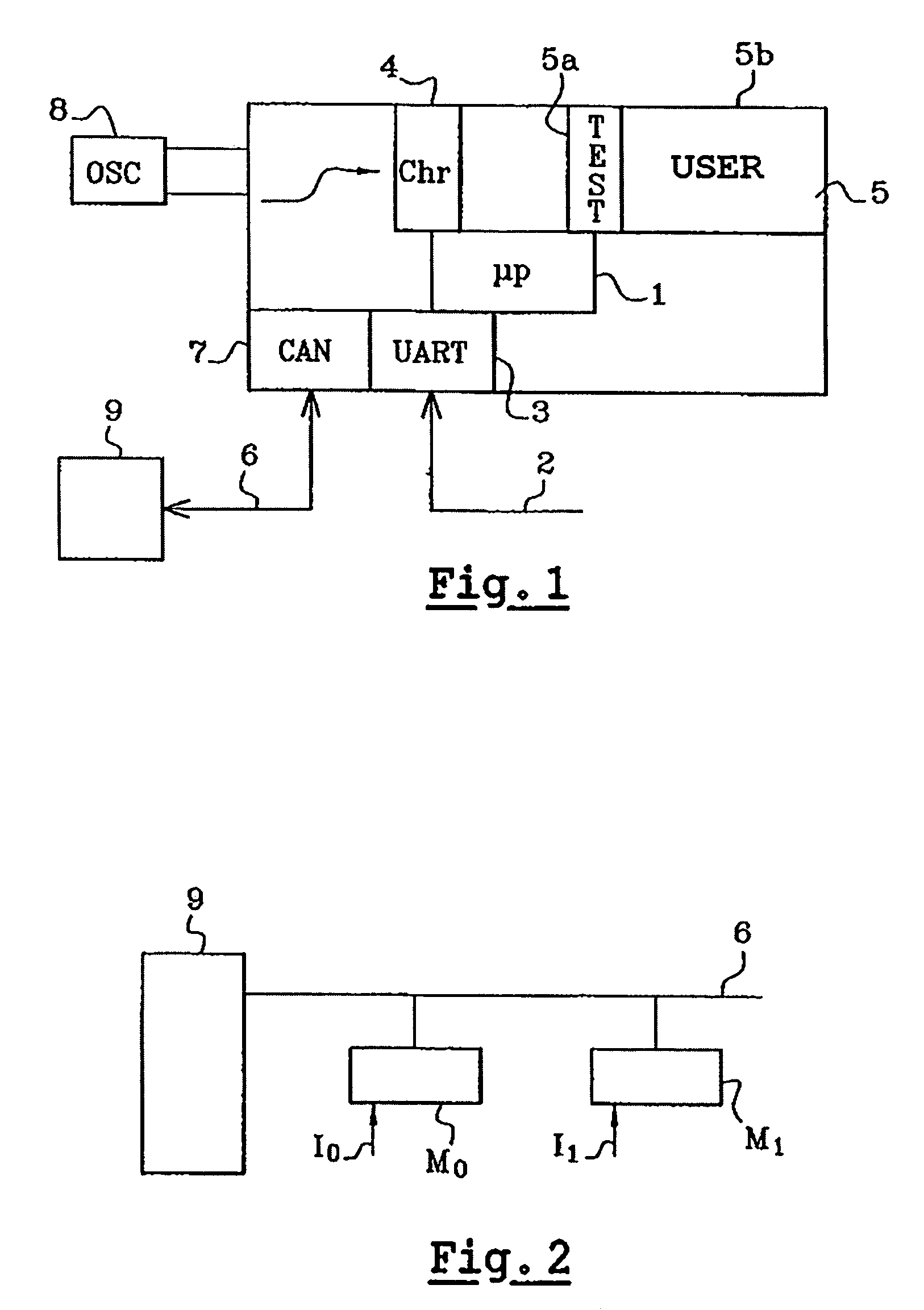
[0035]The integrated hardware resource consisting of the chronometer reference 4 in FIG. 1 is used for everything related firstly to the trigger sequence to be implemented when blank flash memories have to be programmed. The chronometer 4 is activated by a derivative of the internal frequency of the system and its role will be to measure the transmission duration of a predefined frame comprising a predetermined number of binary elements.
[0036]The exact binary throughput on the CAN can be precisely calculated by measuring the transmission duration for a number of transitions through the internal frequency of the system. Thus, the microprocessor 1 can be adapted to the frequency of the CAN. The CAN module 7 of the circuit is then configured to actively participate in the communication.
[0037]Therefore, a first phase will consist of detecting the binary throughput on the CAN.
[0038]Detection of the binary throughput is based on the measurement in time of a predefined frame transmitted on...
PUM
 Abstract
Description
Claims
Application Information