Dendrite growth control circuit

a technology of growth control and dendrite, applied in the direction of semiconductor devices, semiconductor/solid-state device details, electrical devices, etc., can solve the problem of interconnections then impairing circuit functioning

Active Publication Date: 2006-09-19
GLOBALFOUNDRIES U S INC
View PDF8 Cites 10 Cited by
  • Summary
  • Abstract
  • Description
  • Claims
  • Application Information

AI Technical Summary

Problems solved by technology

The shorted interconnects then impair circuit functioning.

Method used


Image

  • Dendrite growth control circuit
  • Dendrite growth control circuit
  • Dendrite growth control circuit

Examples


Embodiment Construction

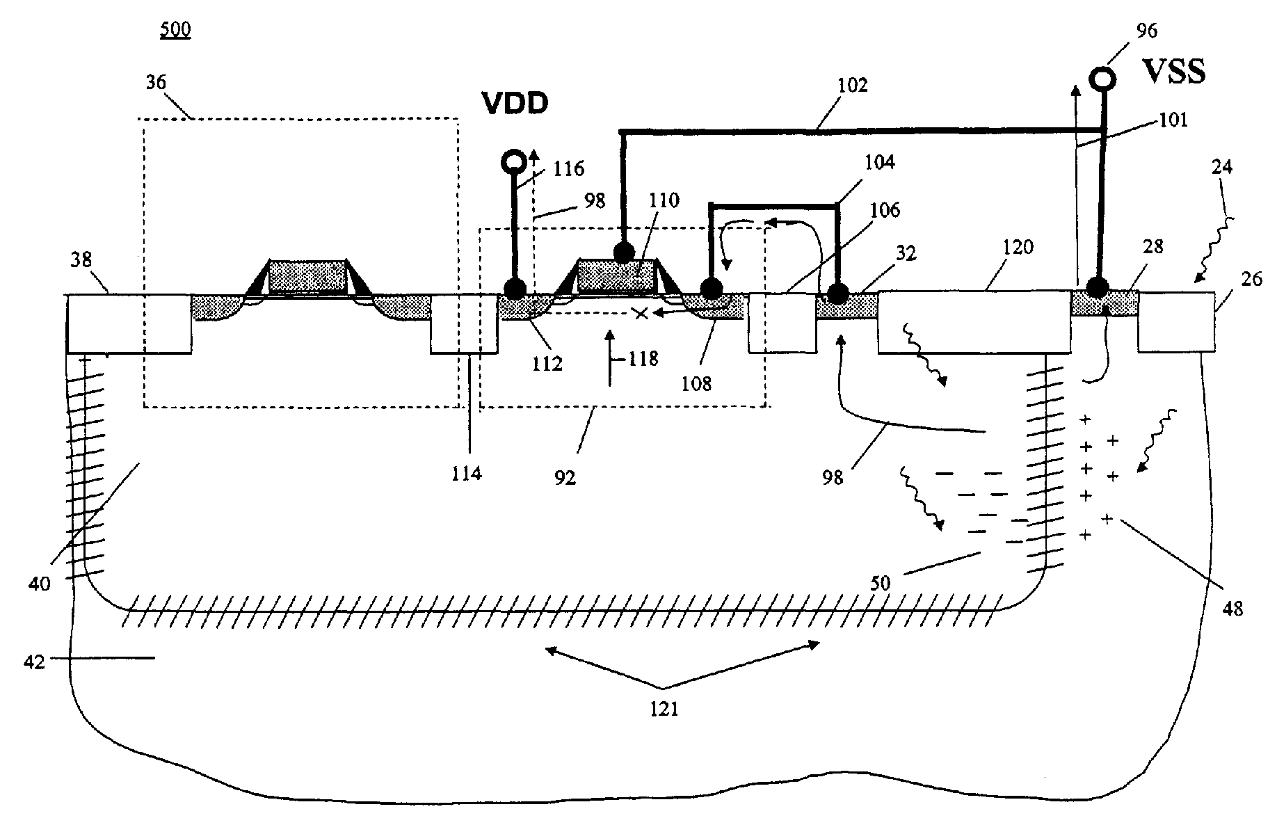
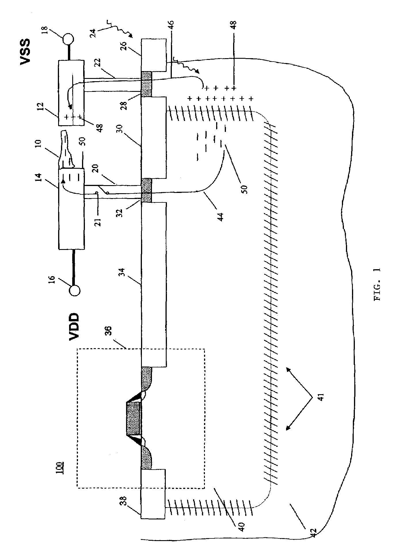
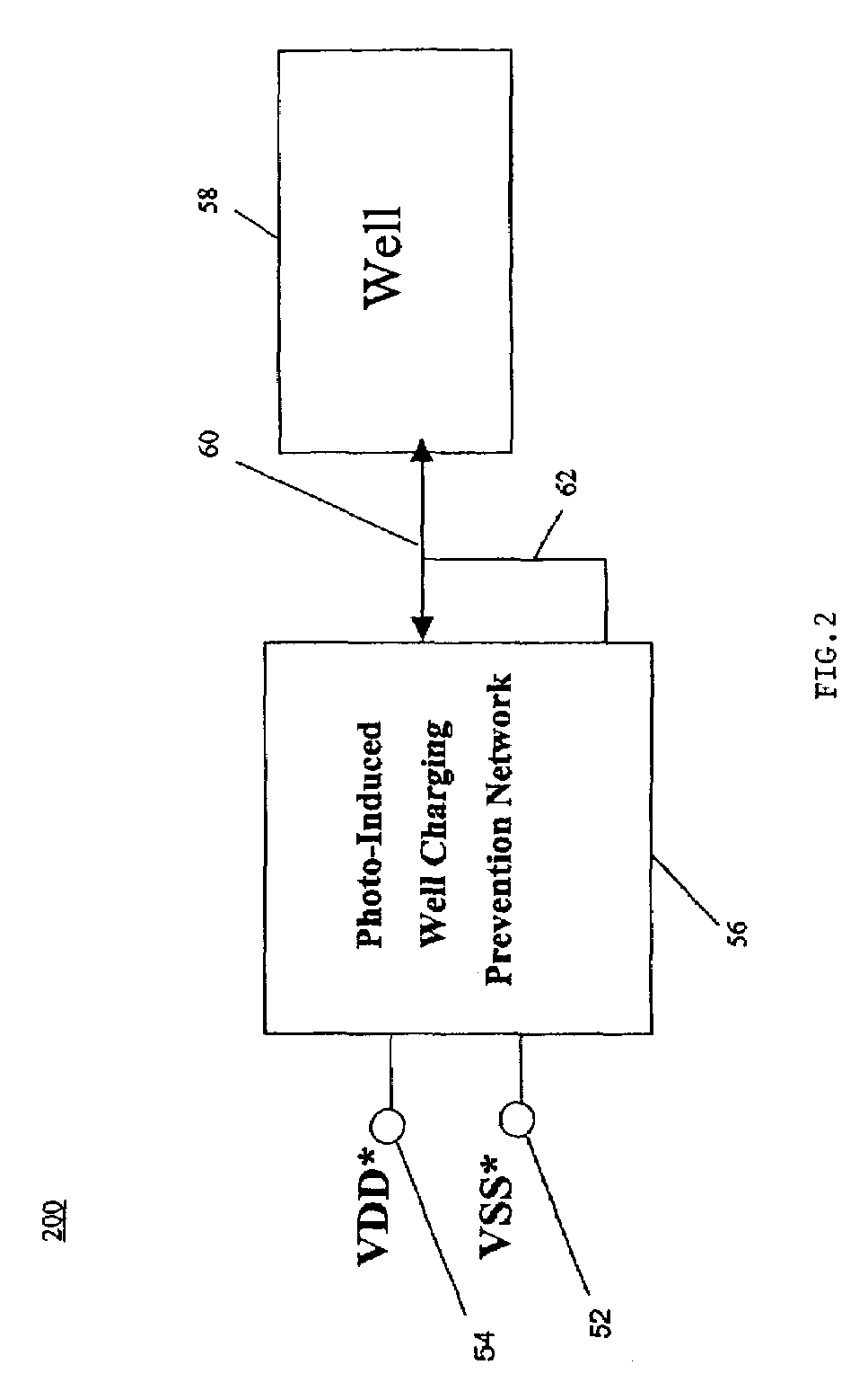
[0020]The invention relates to, for example, a structure and method for controlling or preventing dendrite growth between interconnects during semiconductor fabrication. In the embodiments of the invention, a circuit is provided for breaking the current flow path which contributes to dendrite formation. Thus, by controlling or preventing dendrite formation, it is possible to prevent shorts in the circuit. Accordingly, embodiments of the invention include a circuit, such as a switch or back-to-back diodes, for breaking the current flow path which contributes to dendrite formation while the semiconductor device is being processed. The circuit is configured so that the circuit is open during device fabrication and closed during operation of the semiconductor device. The circuit may be referred alternatively as a “dendrite control network,” a “dendrite control circuit,” a “photo-induced well charging prevention network,” or other similar term which indicates a circuit configured to redu...


PUM


Abstract

A circuit is provided which prevents dendrite formation on interconnects during semiconductor device processing due to a dendrite-forming current. The circuit includes a switch located in at least one of the dendrite-forming current paths. The switch is configured to be open or in the “off” state during processing, and is configured to be closed or in the “on” state after processing to allow proper functioning of the semiconductor device. The switch may include an nFET or pFET, depending on the environment in which it is used to control or prevent dendrite formation. The switch may be configured to change to the “closed” state when an input signal is provided during operation of the fabricated semiconductor device.

Description

FIELD OF THE INVENTION[0001]The invention relates to semiconductor device fabrication, and more particularly to controlling or preventing dendrite growth between interconnects during semiconductor device fabrication.BACKGROUND DESCRIPTION[0002]Under some circumstances, dendrites of conductive material may be formed between metal or other conductive material interconnects during fabrication of a semiconductor device. For example, where copper lines are formed by a damascene process, a polishing step is utilized to planarize the surface of the layer holding the damascene-formed lines. Typically, the polishing step involves a slurry incorporating a grinding compound and / or chemical. The polishing process accordingly will produce small particles of the material being ground away which will remain suspended in the slurry. Consequently, the interconnect being polished will be immersed in a slurry having conductive particles suspended therein.[0003]Under certain conditions, a voltage poten...

Claims


Application Information

Patent Timeline
Patent Type & Authority Patents(United States)
IPC IPC(8): H01L23/48H01L23/52H01L29/40
CPCH01L21/76838
Inventor HERSHBERGER, DOUGLAS B.VOLDMAN, STEVEN H.ZIERAK, MICHAEL J.
Owner GLOBALFOUNDRIES U S INC
Why Eureka
Try Eureka