
Versatile RAM for programmable logic device

a programmable logic and ram technology, applied in the field of systems for data storage on programmable logic devices, can solve the problems of large system resources, large amount of system resources, and large amount of building rams out of these les, and achieve the effects of reducing routing resources, efficiently enabling, and efficiently implementing rams in the pld

Inactive Publication Date: 2006-09-19
ALTERA CORP
View PDF254 Cites 26 Cited by
  • Summary
  • Abstract
  • Description
  • Claims
  • Application Information

AI Technical Summary

Benefits of technology

[0005]It is an advantage of the present invention that it provides an improved circuitry and methods for implementing RAM in a PLD. It is a further advantage of the present invention that it provides improved circuitry and methods for reducing the amount of routing resources required when using relatively extremely wide RAMs.

Problems solved by technology

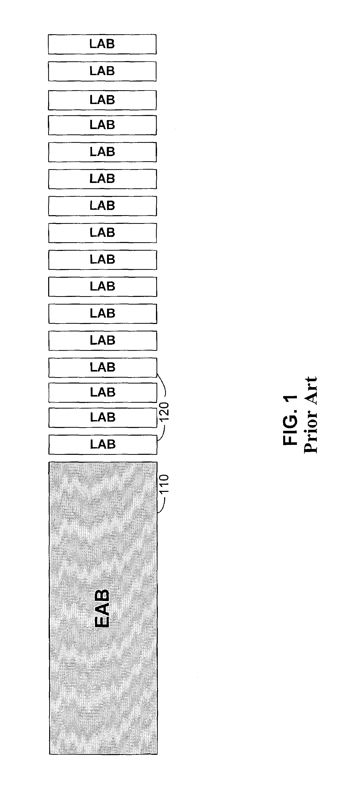
If the only storage elements on a PLD were the register in each of these LEs, then building a RAM out of these LEs would be relatively very expensive (i.e., require a large amount of system resources)—a single 16K bit RAM may consume an entire PLD.
One disadvantage of this solution is that the LUT is no longer available for use as logic, and the amount of extra logic and routing resources required to create RAMs that are deeper than 16 bits (by stitching these smaller blocks together) is still quite expensive.

Method used


Image

  • Versatile RAM for programmable logic device
  • Versatile RAM for programmable logic device
  • Versatile RAM for programmable logic device

Examples


Embodiment Construction

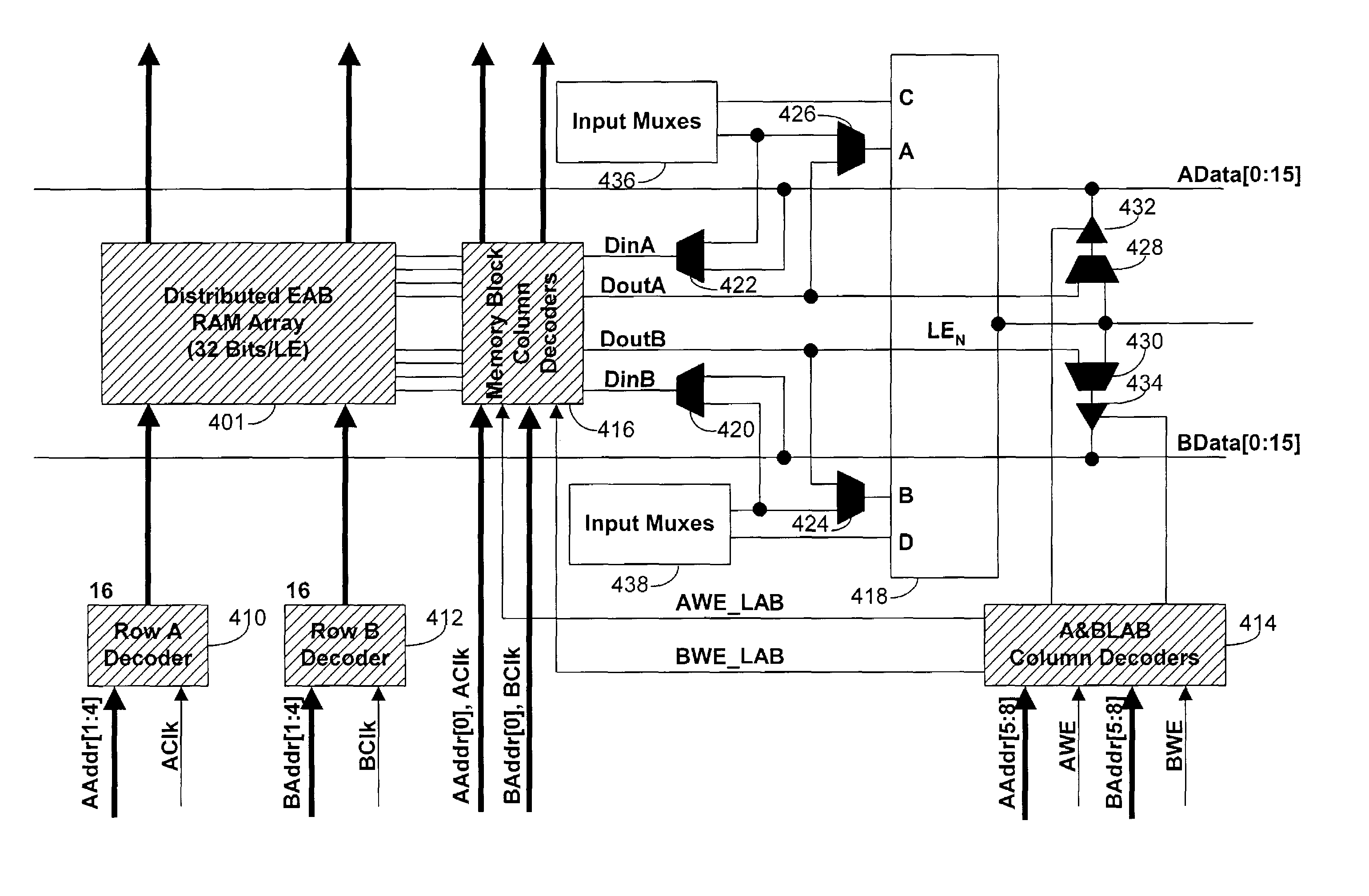
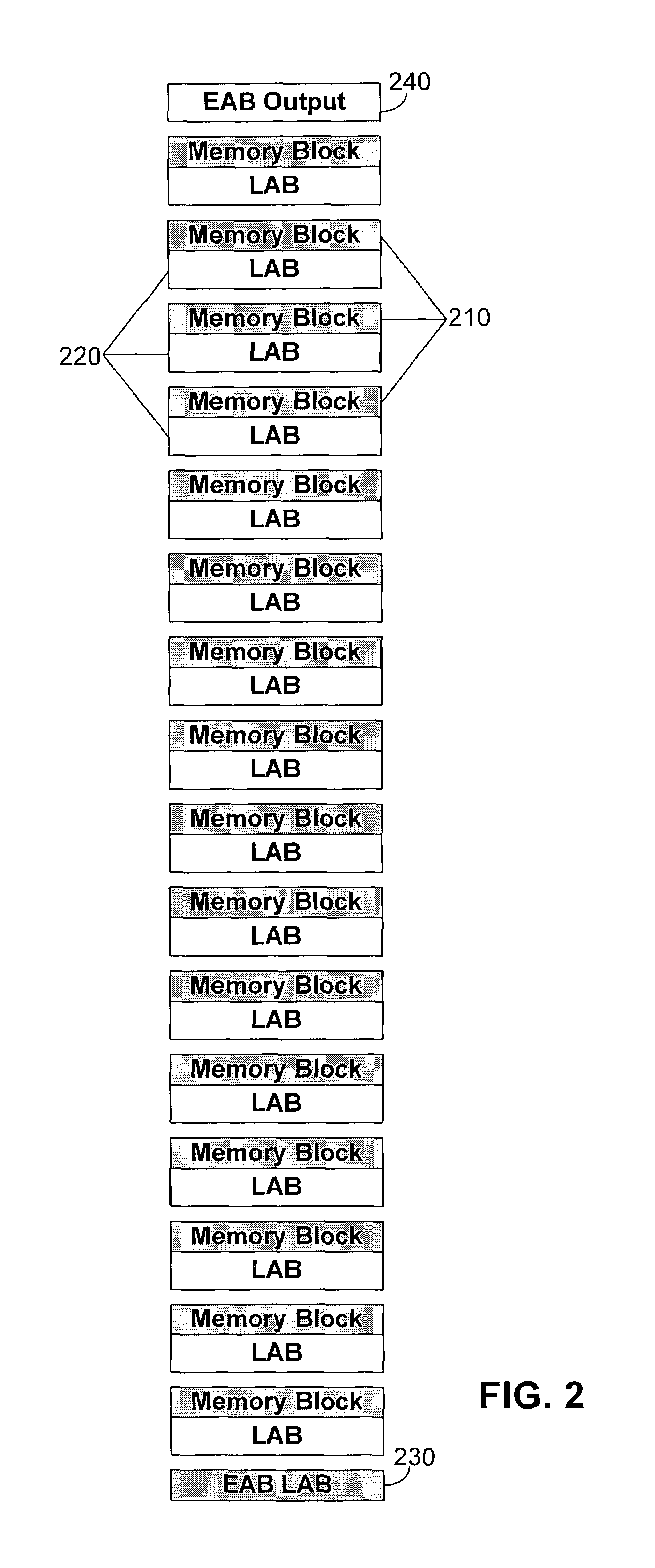
[0017]RAM in a PLD requires addressing to identify the location in memory that is either being written to or read from. As described in the background of the invention, different designs require different memory configurations. The circuits and methods according to the invention preferably distribute memory blocks such that an individual memory block—e.g., 256-bit, dual port (the number of ports being determined by the number of distinct sets of “address” lines that feed the RAM)—may be associated with a single LAB. Furthermore, the circuits and methods according to the invention preferably provide at least two different methods of addressing at least a portion of the addresses in the individual memory blocks. Using a first method of addressing, wherein a single addressing scheme is used, the memory blocks may be conglomerated to operate as a single, large memory block. Using an alternative method, the portions of the resources found in each of the LABs may be used to address the me...


PUM


Abstract

Circuits and methods for providing versatile RAM for a programmable logic device are provided. These circuits and methods preferably allow signal lines that may be used to provide inputs for logic elements to be used instead for addressing memory blocks that form the versatile RAM.

Description

BACKGROUND OF THE INVENTION[0001]This invention relates to methods and systems for data storage on Programmable Logic Devices (PLDs). More particularly, this invention relates to configuring data storage on PLDs in a versatile fashion. U.S. Pat. No. 6,144,573 describes memory circuits and is hereby incorporated by reference herein in its entirety.[0002]Designs that are implemented in Programmable Logic Devices (PLDs) often require RAM blocks of various sizes. Some designs require relatively shallow, wide RAM—e.g., 16 bits wide by 256 words deep—, while some designs require relatively deep, narrow RAM—e.g., 1 bit wide by 4K words deep—, and some designs require an odd mixture of the two.[0003]In order to implement RAM efficiently, PLDs may contain dedicated circuitry for implementing RAM blocks.[0004]It would be desirable to provide an improved circuitry and methods for implementing RAM in a PLD. It would also be desirable to provide circuitry and methods for reducing the amount of r...

Claims


Application Information

Patent Timeline
Patent Type & Authority Patents(United States)
IPC IPC(8): G06F12/00
CPCG11C7/1006H03K19/17728H03K19/1776H03K19/17736H03K19/17732
Inventor PEDERSEN, BRUCE B
Owner ALTERA CORP
Learn More