Microdischarge devices and arrays having tapered microcavities
a micro-cavity and micro-discharge technology, applied in the direction of gas-filled discharge tubes, discharge tubes/lamp details, solid cathodes, etc., can solve the problems of expensive mounting fixtures, fragile quartz or glass envelopes, and bulky devices
- Summary
- Abstract
- Description
- Claims
- Application Information
AI Technical Summary
Problems solved by technology
Method used
Image
Examples
examples
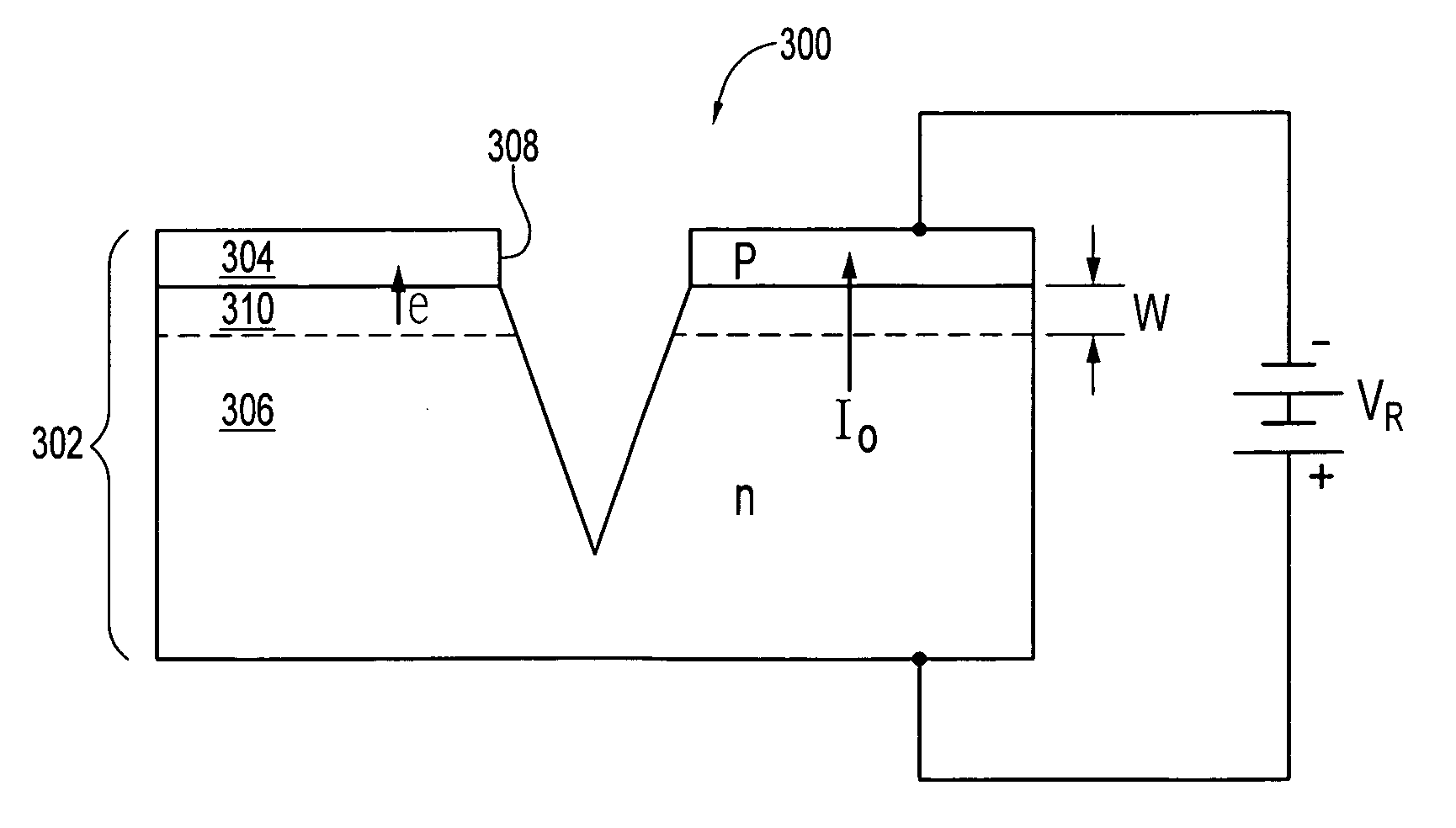
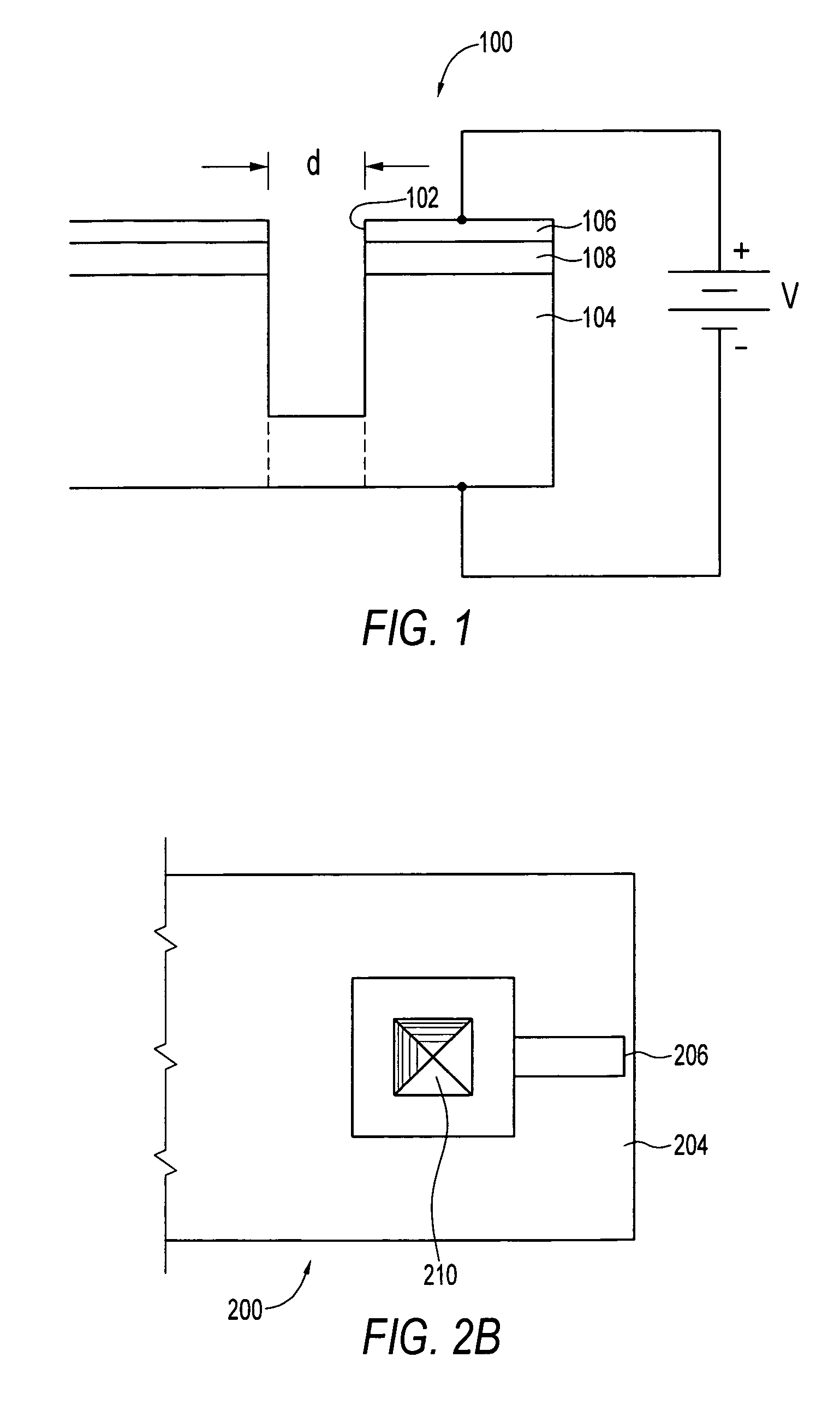
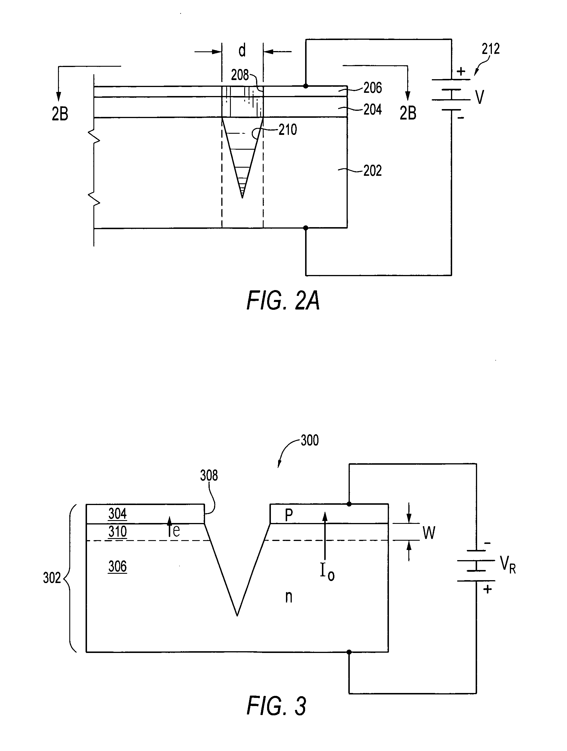
[0071]Devices were fabricated in p-type silicon (100) wafers having a resistivity of 6–8 Ω-cm and a typical thickness of 300 μm. Pyramidal cavities, 50 or 100 μm square at the base and of 35 μm or 70 μm depth, respectively, were fabricated. The cavities were produced by anisotropic wet etching in a 33% (wt / wt) solution of KOH in water. Subsequently, the device dielectric was formed by spin coating an approximately 7.5–8 μm thick layer of a dry etchable polyimide (Dupont 2611, relative permittivity ∈r=2.9) onto the silicon surface followed by curing the polymer at 300° C. in a N2 atmosphere. Subsequently, a 1200–2400 Å thick Ni film was e-beam evaporated onto the polyimide to serve as the anode. The discharge channels in the metal anode and dielectric films were defined photolithographically with a Cr mask and etched by wet and reactive ion etched (O2 plasma) processes, respectively. Some devices additionally had SiO2 or Si3N4 films of about 1500 Å thickness sandwiched between the si...
PUM
 Abstract
Description
Claims
Application Information


