
Process tape for cleaning or processing the edge of a semiconductor wafer

a technology of processing tape and semiconductor wafer, which is applied in the direction of edge grinding machine, grinding machine components, manufacturing tools, etc., can solve the problems of inoperable devices on the wafer, inability to clean or prepare the edge of the semiconductor wafer, and inability to clean the surface of the wafer

Active Publication Date: 2006-10-03
LAM RES CORP
View PDF26 Cites 47 Cited by
  • Summary
  • Abstract
  • Description
  • Claims
  • Application Information

AI Technical Summary

Benefits of technology

[0010]Broadly speaking, the present invention fills these needs by providing an improved substrate bevel and exclusion zone cleaning mechanism. It should be appreciated that the present invention c

Problems solved by technology

If particles or films are left on the surface of the wafer without removing them, the unwanted residual particles or material may cause defects on the wafer surface and inappropriate interactions between metallization features or with subsequent lithography operations.
Such defects may cause devices on the wafer to become inoperable.
Standard brush scrubbing techniques often fail to clean and remove the metal edge beading and loose particles from wafer edge surfaces including the bevel edge and exclusion zone which extends from about 1 to 3 millimeters from the bevel.
Although sufficient center cleaning is performed using roller brushes, not enough mechanical scrubbing is performed at the edge.
Consequently, unwanted material may remain even after repeated conventional brush cleaning.
Unfortunately, prior art wafer edge cleaners must be replaced periodically, increasing operating costs.
Furthermore, the prior art devices have a small area of contact between the cleaning implement and the wafer.
The small area of contact results in reduced efficiency in cleaning, requiring longer cleaning times.

Method used


Image

  • Process tape for cleaning or processing the edge of a semiconductor wafer
  • Process tape for cleaning or processing the edge of a semiconductor wafer
  • Process tape for cleaning or processing the edge of a semiconductor wafer

Examples


Embodiment Construction

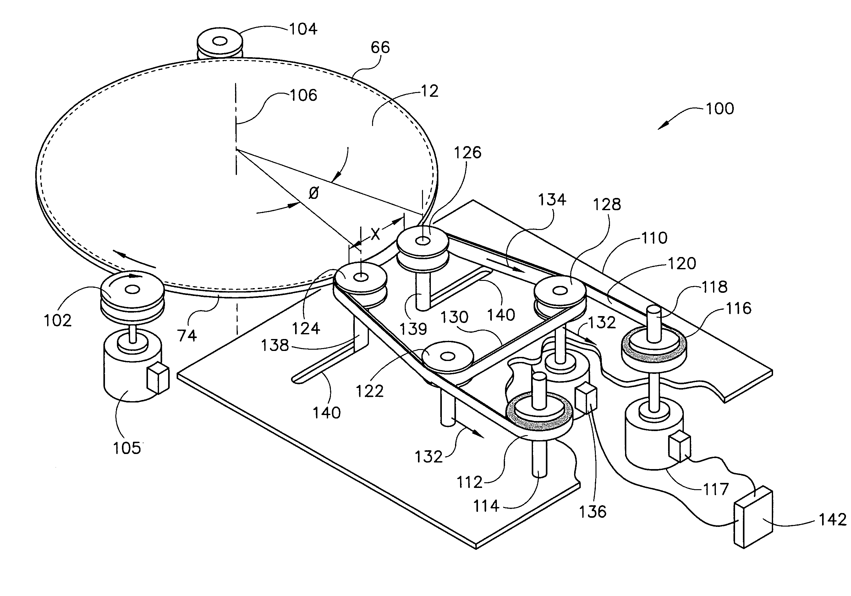
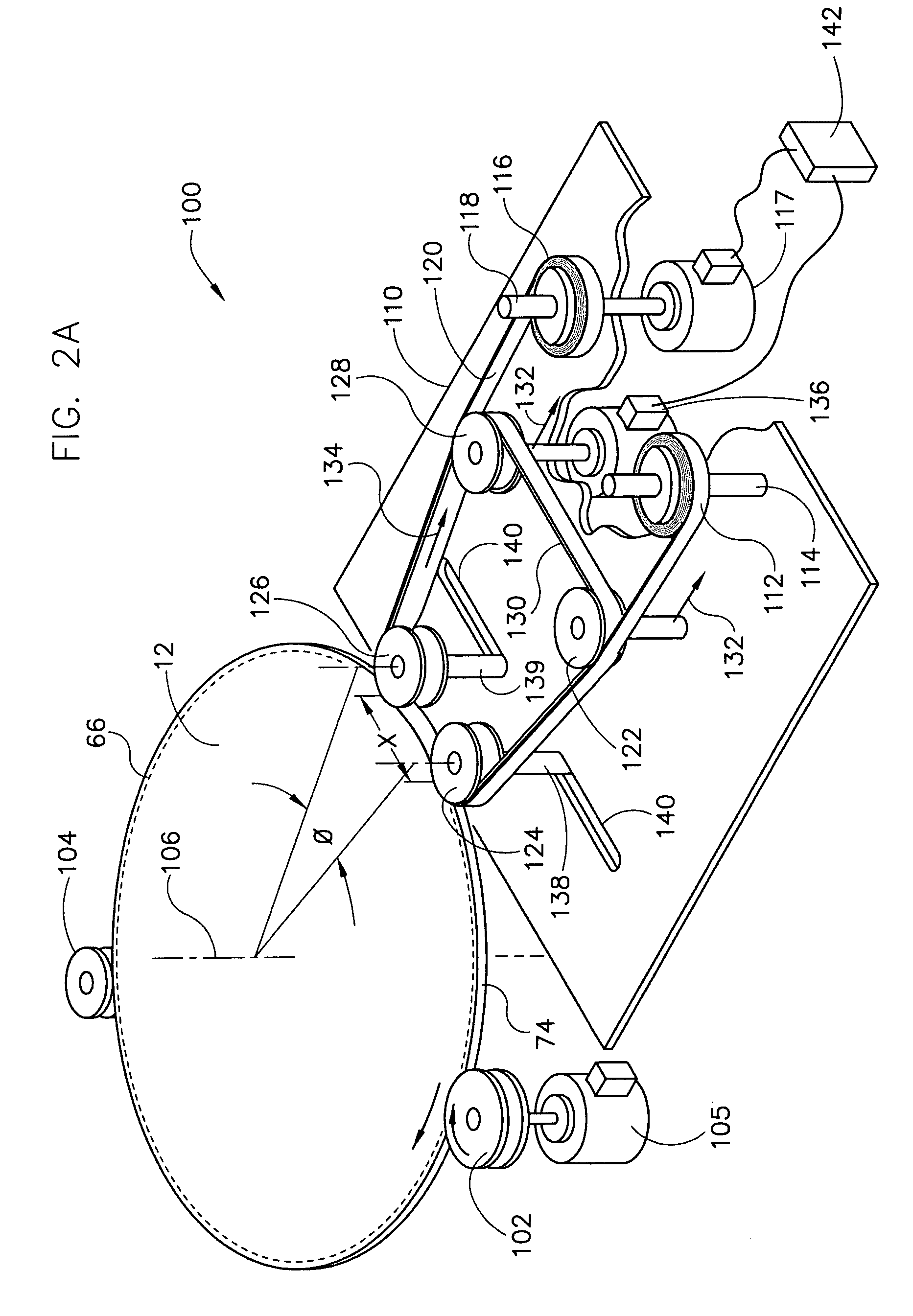
[0022]Several exemplary embodiments for wafer bevel and exclusion zone cleaning system are described below. It will be apparent to those skilled in the art that the present invention may be practiced without some or all of the specific details set forth herein.

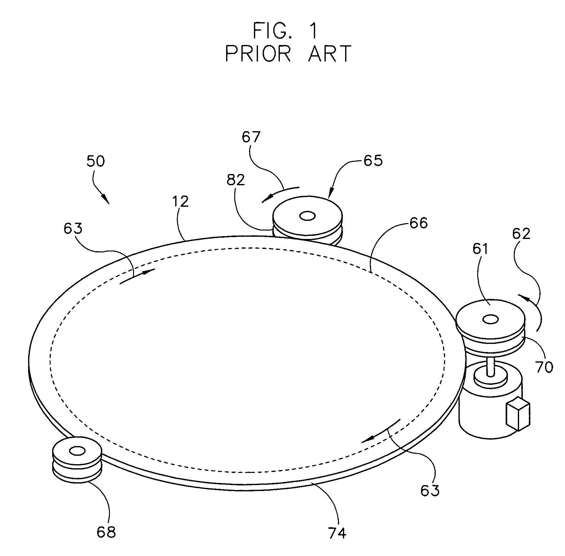
[0023]FIG. 2A shows one embodiment of an edge cleaning apparatus 100. Cleaning apparatus 100 comprises a plurality of rollers to support and rotate wafer 12. Any number of rollers may be used. In one embodiment, driver roller 102 and stator roller 104 engages wafer bevel 74 to support wafer 12. As used herein, the wafer bevel 74 is defined to include the wafer edge surface. As the edge of the wafer has a surface that is sometimes somewhat rounded or curved, the edge can extend up to or past the curved portions and onto the flat surface of either or both of the top and bottom of the wafer. The flatter surfaces near the edge are referred to as the edge region 66 and include what is commonly referred to as the exclusion zone. The...


PUM

PropertyMeasurementUnit
Areaaaaaaaaaaa
Tensionaaaaaaaaaa

Abstract

A wafer bevel processing apparatus comprises a plurality of rollers for rotatably supporting a wafer, first process roller, a second process roller, and a process tape extending between the first process roller and the second process roller. The first and second process rollers are positioned to cause the process tape to contact an edge of the wafer when the wafer is loaded into the processing apparatus. The process tape is configured to frictionally prepare the edge where contact occurs with the process tape.

Description

BACKGROUND OF THE INVENTION[0001]1. Field of the Invention[0002]The present invention relates generally to semiconductor wafer cleaning and preparation, and more particularly, to a method and apparatus for cleaning or preparing wafer edges after various fabrication operations.[0003]2. Description of the Related Art[0004]In the field of semiconductor chip fabrication processing, it is well known that there is a need to clean a semiconductor substrate wafer where a fabrication operation has been performed that leaves unwanted residuals on the surface of the wafer. Examples of such fabrication operations include plasma etching, material depositions and chemical mechanical planarization (CMP). CMP is commonly performed on both dielectric materials and conductive materials such as oxide and copper. If particles or films are left on the surface of the wafer without removing them, the unwanted residual particles or material may cause defects on the wafer surface and inappropriate interacti...

Claims


Application Information

Patent Timeline
IPC IPC(8): B24B1/00
CPCB24B9/065B24B41/067
Inventor OWCZARZ, ALEKSANDER
Owner LAM RES CORP
Features
  • Generate Ideas
  • Intellectual Property
  • Life Sciences
  • Materials
  • Tech Scout
  • Unparalleled Data Quality
  • Higher Quality Content
  • 60% Fewer Hallucinations
Learn More