Process for preparing a substantially transparent conductive layer configuration

a technology of substantially transparent conductive layer and composite layer, which is applied in the direction of photoprinting process, diazo-type process, non-conductive material with dispersed conductive material, etc., can solve the problems of short circuit and long term of electrodes, and achieves convenient application, high conductivity, and improved flatness

Inactive Publication Date: 2006-10-10
AGFA GEVAERT AG
View PDF17 Cites 9 Cited by
  • Summary
  • Abstract
  • Description
  • Claims
  • Application Information

AI Technical Summary

Benefits of technology

[0018]It has been surprisingly found that a thin substantially transparent conductive layer with high conductivity and with an outermost surface with improved flatness can be realized in a layer containing an intrinsically conductive polymer, e.g. PEDOT / PSS, and a conductive metal, e.g. silver, non-uniformly distributed therein to which functional layers can be readily applied.
[0019]Upon applying a potential between the conductive layer, according to the present invention, as cathode and a counter-electrode as cathode under conditions of high relative humidity metal ions present at the anode, there always being an equilibrium between metal ions and metal atoms, diffuse under the applied potential to the cathode, where they are deposited at metal atoms which stack forming dendritic metal which grow towards the anode. This results long term in short circuiting of the electrodes.

Problems solved by technology

This results long term in short circuiting of the electrodes.

Method used


Image

  • Process for preparing a substantially transparent conductive layer configuration
  • Process for preparing a substantially transparent conductive layer configuration
  • Process for preparing a substantially transparent conductive layer configuration

Examples


example 2 (

INVENTION)

Preparation of the Palladium Sulphide Dispersion:

[0148]The preparation of the physical development nuclei (PdS) is described in the example of EP-A 0769 723. From this example solutions A1, B1 and C1 were used to prepare the nuclei.

Preparation of Material D:

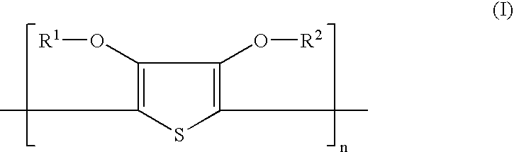
[0149]100 g of the above-described PEDOT / PSS dispersion was mixed with 3.35 g of the PdS-dispersion. To this mixture, 1.25 g of a 10 g / L water solution of AEROSOL™ OT (American Cyanamid), 0.625 g of a 50 g / l solution of perfluorcaprylamidpolyglycol and 61.9 ml of water were added to give the coating dispersion. This dispersion was coated on a support consisting of a poly(ethylene terephthalate) film and a 4 μm thick gelatin subbing layer to a wet-layer thickness of 50 μm with a doctor blade and then dried for 15 minutes at 100° C. to produce Material D.

Preparation of the Transfer Emulsion Layer:

[0150]The preparation of the silver chlorobromide emulsion and the preparation of the transfer emulsion layer was as disclosed ...

example 3 (

INVENTION)

[0157]Conceptual experiments were carried out with a recorder film with a gelatine to silver ratio of 0.014. Exposed areas of 1×3 cm2 as electrodes with a separation of 40 μm gave conducting silver patterns upon processing by conventional graphic processing. The resulting electrode pattern had a surface resistance of 50 to 100 ohm / square.

[0158]These electrodes were conditioned for 3 days at 35° C. and a relative humidity of 80%. The aqueous solutions used for treating the electrodes prior to applying a potential of 100 V between neighbouring electrodes are listed in Table 3.

[0159]

TABLE 3SolutionSolutionnr.active ingredientconc. (%]solvent1STAB01 (1-phenyl-5-mercapto-tetrazole)1.0water*2STAB010.1water*3STAB01 + Antarox ™ CO 630#1.0 + 0.5water4STAB01 + Antarox ™ CO 630#0.1 + 0.5water5STAB02 (sodium tartrate)10water6STAB02 (sodium tartrate)1water7STAB03 (thiourea)10water8STAB03 (thiourea)1water9STAB04 (sodium sulphide)10water10STAB04 (sodium sulphide)1water11STAB05 (5-methyl-...


PUM

PropertyMeasurementUnit
weight ratioaaaaaaaaaa
diameteraaaaaaaaaa
surface resistivityaaaaaaaaaa

Abstract

A substantially transparent conductive layer on a support, the layer comprising an intrinsically conductive polymer e.g. containing an intrinsically conductive polymer optionally containing structural units represented by formula (I):wherein n is larger than 1 and each of R1 and R2 independently represents hydrogen or an optionally substituted C1-4 alkyl group or together represent an optionally substituted C1-4 alkylene group or an optionally substituted cycloalkylene group, preferably an ethylene group, an optionally alkyl-substituted methylene group, an optionally C1-12 alkyl- or phenyl-substituted ethylene group, a 1,3-propylene group or a 1,2-cyclohexylene group; and a conductive metal non-uniformly distributed therein and forming of itself a conductive entity; a process for preparing the transparently conductive layer; and light emitting diodes, photovoltaic devices, transistors and electroluminescent devices comprising the above-described conductive layer.

Description

[0001]This application claims the benefit of U.S. Provisional Application No. 60 / 418,637 filed Oct. 15, 2002, which is incorporated by reference. In addition, this application claims the benefit of International Application No. PCT / EP 02 / 09427 filed Aug. 22, 2002, which is also incorporated by reference.FIELD OF THE INVENTION[0002]The present invention relates to a single layer composite substantially transparent conductive layer.BACKGROUND OF THE INVENTION[0003]In many applications there is a requirement for inexpensive transparent conducting layers, but a busbar will be also required for some of the (large area) applications. Highly conductive (non-transparent) patterns can be made by screen-printing conducting pastes such as silver or carbon black pastes. Vacuum evaporation of metals through shadow masks is another method. Yet another method makes use of homogeneous conductive metallized surfaces which can be patterned by use of photoresist technology in combination with a metal ...

Claims


Application Information

Patent Timeline
Patent Type & Authority Patents(United States)
IPC IPC(8): G03C1/04G03C5/26G03C8/28G03C8/32H01C13/00C08G61/12G03C1/035G03C1/047G03C1/89H01B1/12H01L51/00H01L51/30
CPCC08G61/126G03C1/89H01B1/127H01L51/0021H01L51/0037H01G11/48G03C1/035G03C1/047H01L51/445G03C2007/3025G03C2200/27Y02E10/549Y02E60/13H10K71/60H10K85/1135H10K30/83
Inventor ANDRIESSEN, HIERONYMUS
Owner AGFA GEVAERT AG
Why Eureka
Try Eureka