Sample inspection system

a technology of sample inspection and inspection system, which is applied in the field of sample inspection system, can solve the problems of surface breaking defects in semiconductor wafers, potential detriment to the performance of semiconductor chips made from wafers with such defects, and surface breaking defects in wafers, so as to reduce the position error of spots

Inactive Publication Date: 2006-10-10
KLA TENCOR TECH CORP
View PDF65 Cites 20 Cited by
  • Summary
  • Abstract
  • Description
  • Claims
  • Application Information

AI Technical Summary

Benefits of technology

[0009]Another aspect of the invention is directed towards an optical system for detecting anomalies of a sample, comprising means for directing at least one beam of radiation along a path onto a spot on a surface of the sample; a first detector and means for receiving scattered radiation from the sample surface and originating from the at least one beam and for focusing the scattered radiation to said first detector for sensing anomalies. The system further comprises a second, position sensitive, detector detecting a specular reflection of said at least one beam in order to detect any change in height of the surface at a spot; and means for altering the path of the at least one beam in response to the detected change in height of the surface of the spot to reduce position error of the spot caused by change in height of the surface of the spot.
[0015]Another aspect of the invention is directed towards an optical method for detecting anomalies of a sample, comprising directing at least one beam of radiation along a path onto a spot on the surface of the sample; collecting scattered radiation from the sample surface and originating from the at least one beam, and focusing the collected scattered radiation to a first detector for sensing anomalies. The method further comprises detecting a specular reflection of said at least one beam in order to detect any change in height of the surface at the spot and altering the path of the at least one beam in response to the detected change in height of the surface of the spot to reduce position error of the spot caused by change in height of the surface of the spot.

Problems solved by technology

COPs are surface breaking defects in semiconductor wafers which have been classified as particles due to inability of conventional inspection systems to distinguish them from real particles.
Another issue which has great significance in wafer inspection is that of COPs.
These are surface-breaking defects in the wafer.
According to some opinions in the wafer inspection community, such defects can cause potential detriments to the performance of semiconductor chips made from wafers with such defects.

Method used


Image

  • Sample inspection system
  • Sample inspection system
  • Sample inspection system

Examples


Embodiment Construction

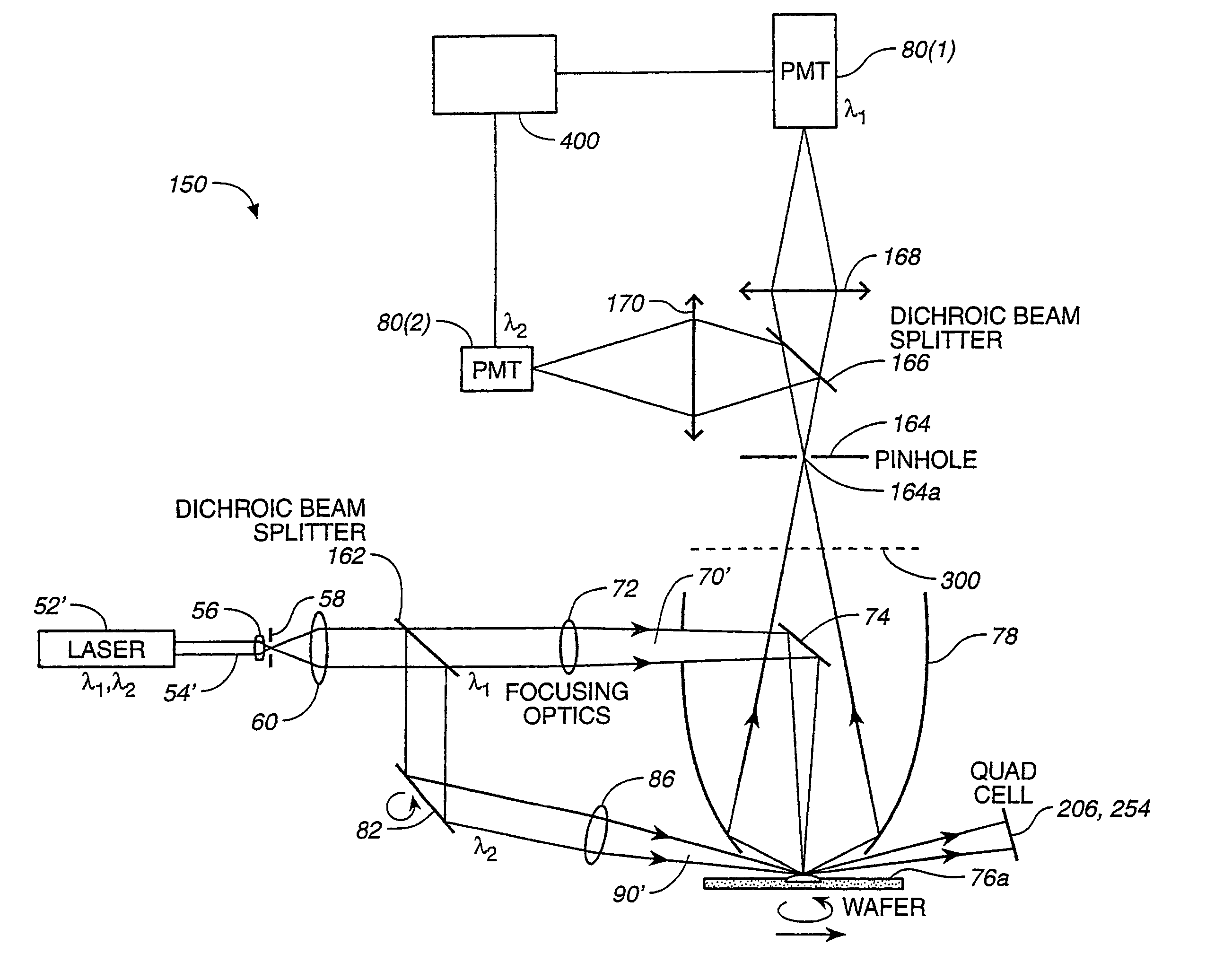
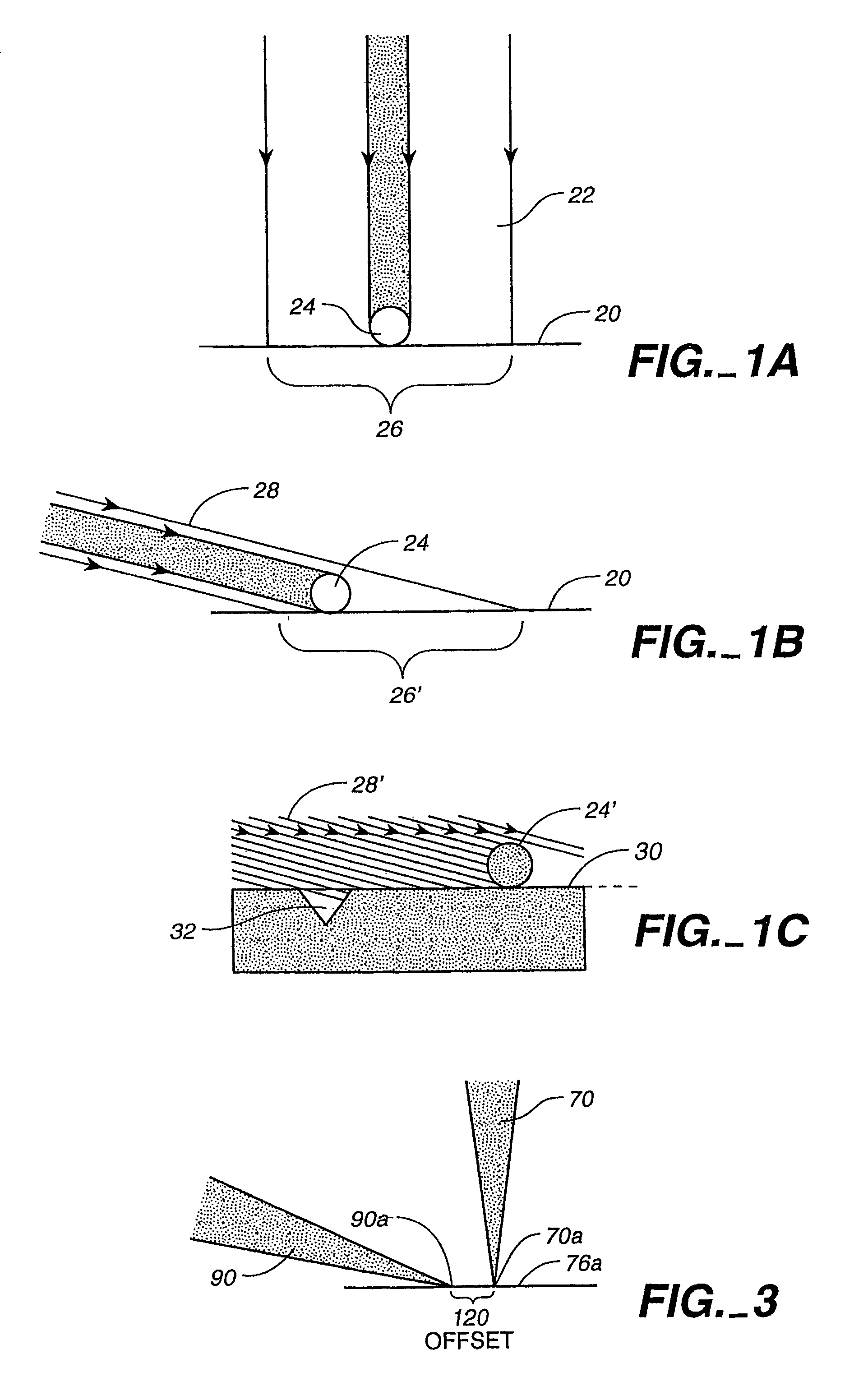
[0032]FIG. 1A is a schematic view of a surface 20 of a sample to be inspected and an illumination beam 22 directed in a direction normal to surface 20 to illuminate the surface and a particle 24 on the surface. Thus, the illumination beam 22 illuminates an area or spot 26 of surface 20 and a detection system (not shown) detects light scattered by particle 24 and by portion or spot 26 of the surface 20. The ratio of the photon flux received by the detector from particle 24 to that from spot 26 indicates the sensitivity of the system to particle detection.

[0033]If an illumination beam 28 directed at an oblique angle to surface 20 is used to illuminate spot 26′ and particle 24 instead, as shown in FIG. 1B, from a comparison between FIGS. 1A and 1B, it will be evident that the ratio of the photon flux from the particle 24 to that from the illuminated spot will be greater in the case of the oblique illumination in FIG. 1B compared to that in FIG. 1A. Therefore, for the same throughput (s...


PUM

PropertyMeasurementUnit
angleaaaaaaaaaa
angleaaaaaaaaaa
wavelengthaaaaaaaaaa

Abstract

A curved mirrored surface is used to collect radiation scattered by a sample surface and originating from a normal illumination beam and an oblique illumination beam. The collected radiation is focused to a detector. Scattered radiation originating from the normal and oblique illumination beams may be distinguished by employing radiation at two different wavelengths, by intentionally introducing an offset between the spots illuminated by the two beams or by switching the normal and oblique illumination beams on and off alternately. Beam position error caused by change in sample height may be corrected by detecting specular reflection of an oblique illumination beam and changing the direction of illumination in response thereto. Butterfly-shaped spatial filters may be used in conjunction with curved mirror radiation collectors to restrict detection to certain azimuthal angles.

Description

CROSS-REFERENCE TO RELATED APPLICATIONS[0001]This application is a continuation of U.S. patent application Ser. No. 10 / 671,261, filed Sep. 24, 2003, now abandoned; which is a continuation of U.S. patent application Ser. No. 09 / 746,141, filed Dec. 21, 2000, now U.S. Pat. No. 6,639,662; which is a continuation of U.S. patent application Ser. No. 08 / 933,771, filed Sep. 19, 1997, now U.S. Pat. No. 6,201,601; which applications are incorporated herein in their entireties by this reference.BACKGROUND OF THE INVENTION[0002]This invention relates in general to sample inspection systems and, in particular, to an improved inspection system with good sensitivity for particles as well as crystal-originated-particles (COPs). COPs are surface breaking defects in semiconductor wafers which have been classified as particles due to inability of conventional inspection systems to distinguish them from real particles.[0003]Systems for inspecting unpatterned wafers or bare wafers have been proposed. Se...

Claims


Application Information

Patent Timeline
Patent Type & Authority Patents(United States)
IPC IPC(8): G01N21/00G01N21/47G01N21/95
CPCG01N21/47G01N21/9501G01N21/956
Inventor VAEZ-IRAVANI, MEHDISTOKOWSKI, STANLEYZHAO, GUOHENG
Owner KLA TENCOR TECH CORP
Why Eureka
Try Eureka