Method for testing OLED substrate and OLED display

a technology of oled substrate and oled display, which is applied in the direction of identification means, instruments, process and machine control, etc., can solve the problems of uniformity of display across the whole screen, and non-uniformity of oled elements made by local heating with laser irradiation

Active Publication Date: 2006-10-17
INNOLUX CORP
View PDF13 Cites 20 Cited by
  • Summary
  • Abstract
  • Description
  • Claims
  • Application Information

AI Technical Summary

Benefits of technology

[0019]The method for testing an OLED substrate according to the present invention can determine a current value passing through OLED elements via each switching element using a small amount of data, which leads to learn the distribution status of the current of the whole OLED substrate. It is possible to obtain the electron mobility and the threshold voltage of each switching element by changing the level of the first pulse signal to be provided to the above-mentioned selection signal lines against the signal level to be provided to the data signal lines.

Problems solved by technology

Thin film transistors made from amorphous silicon do not have so remarkable nonuniformity in characteristics, so that unevenness of display is dispersed to the whole screen.
On the contrary, polysilicon made by local heating with laser irradiation tends to have non-uniform characteristics per unit of pixel.
These switching elements cause non-uniform luminance in OLED elements due to non-uniform characteristics.
As a result, display quality is uneven.
However, the number of switching elements is dramatically increased when the display size gets bigger.
Consequently, it is difficult to improve characteristics of all switching elements.
Displays targeted for displaying moving picture become extremely deteriorated in picture quality when nonuniformity of emitted light luminance is locally concentrated on the screen.
This raised a problem of high costs for additional circuits.
Accordingly, there was a problem that the circuit of the display became complicated.
Moreover, the display needs a long test time for testing all pixels and a large-capacity memory to store data.

Method used


Image

  • Method for testing OLED substrate and OLED display
  • Method for testing OLED substrate and OLED display
  • Method for testing OLED substrate and OLED display

Examples


example 1

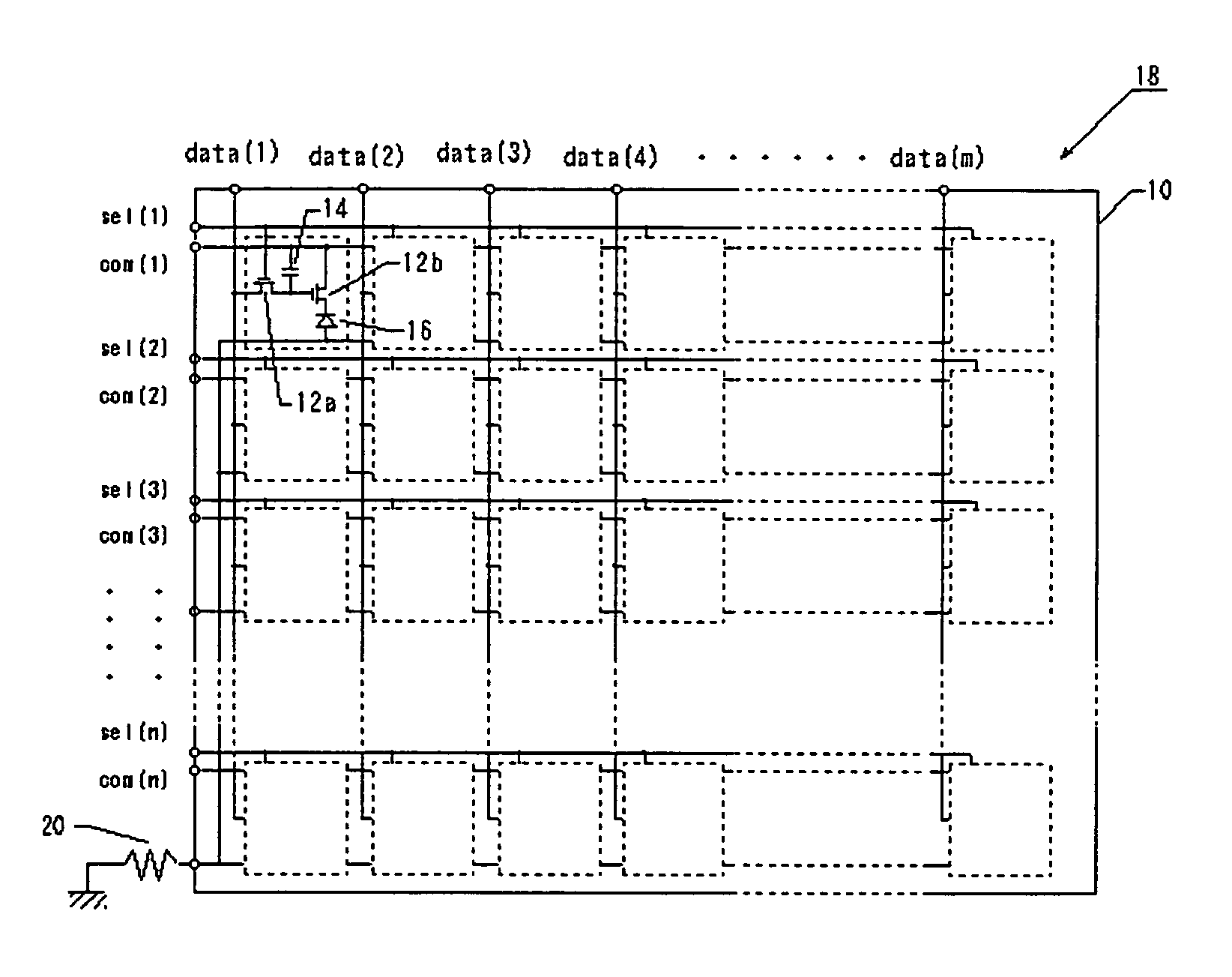
[0036]Preferred embodiments of the present invention are described below. FIG. 1 shows an OLED display and the reference character 10 is an insulating substrate, the reference characters 12a and 12b are a pair of first and second switching elements (MOSFET shown in the figure). A gate electrode of the first switching element 12a is referred to as a selection terminal. And a source electrode is referred to as a data terminal for providing data. A drain electrode is connected to a gate electrode of the second switching element 12b. The reference character 14 is a condenser for data retention whose one end is connected to a connection point of the first switching element 12a and the second switching element 12b.

[0037]The other end of the condenser 14 is connected to the source electrode of the second switching element 12b to be a common terminal. The reference character 16 is an OLED element wherein a cathode electrode is connected to the drain electrode of the second switching element...

example 2

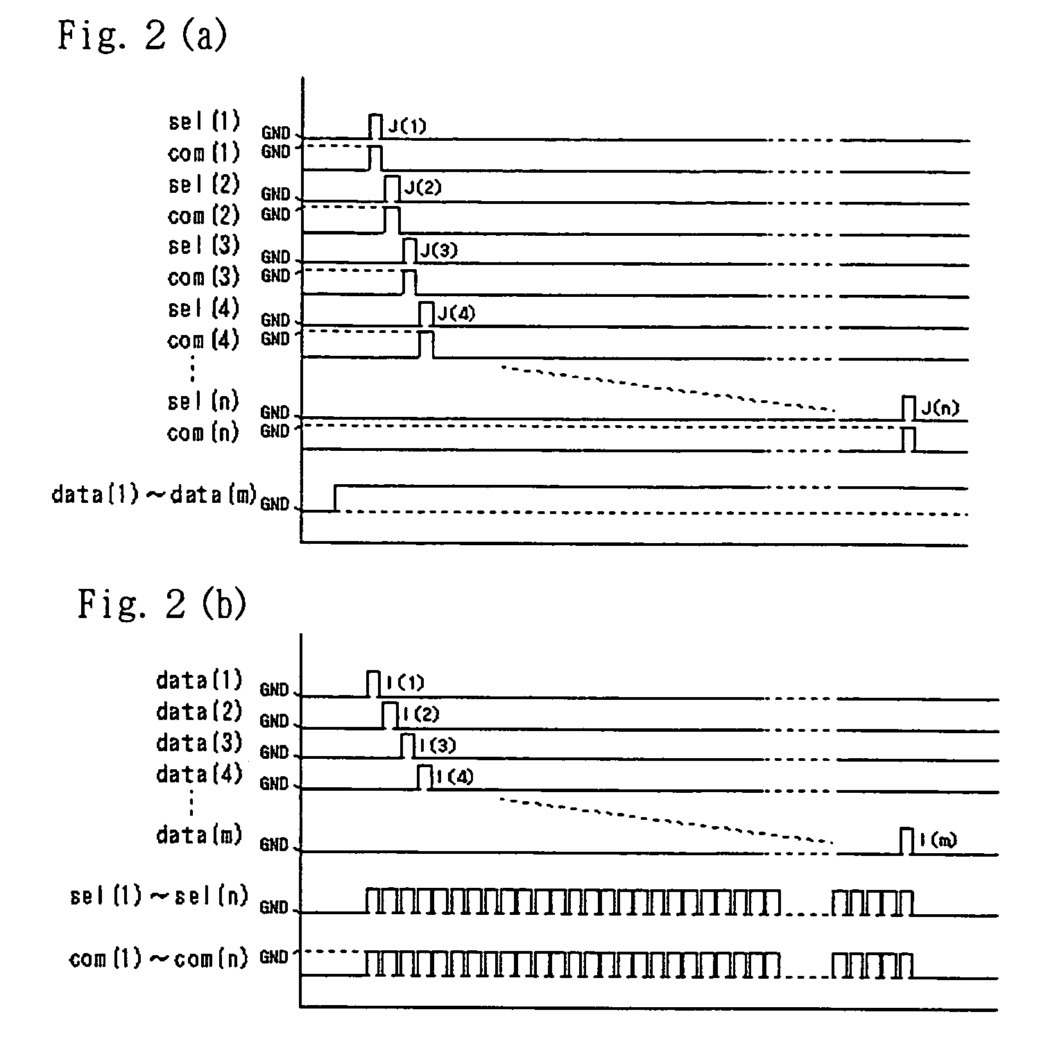
[0043]A pulse signal shown in FIG. 2(a) is provided to an OLED display substrate 18 shown in FIG. 1. A first pulse signal (level: Vg1) is provided to respective selection signal lines sel (1) to sel (n) sequentially while proving all data signal lines data (1) to data (m) with a predetermined level of signal and then a second pulse signal is sequentially provided to common control lines com (1) to com (n) in synchronization between the first and second pulse signals. This applies a voltage in accordance with the difference of the signal provided to the first pulse signal and the data signal line between the gate / source of the switching element 12a. Each time the first and the second pulse signals are provided, current values J1 (1) to J1 (n) passing through the switching element group connected to the selection signal lines sel (1) to sel (n) are obtained.

[0044]A pulse signal shown in FIG. 2(b) is provided. A third pulse signal is provided to the data signal lines data (1) to data (...


PUM


Abstract

A method for testing an OLED substrate comprises: the first step of obtaining a first current value passing through a switching element group connected to a selection signal line; the second step of obtaining a second current value passing through a switching element group connected to a data signal line; and the third step of operating a current passing through each switching element including an OLED element from the current value for each pulse signal obtained by each of the steps 1 and 2.

Description

BACKGROUND OF THE INVENTION[0001]1. Field of the Invention[0002]The present invention relates to a method for testing respective characteristics of a plurality of switching elements arranged on an OLED (Organic Light Emitting Diode) substrate and an OLED display equipped with means for correcting non-uniform characteristics of each switching element.[0003]2. Description of Related Art[0004]An OLED display has an OLED substrate having elements and wiring arranged on an insulating substrate. More particularly, in an OLED display, a plurality of switching elements and OLED elements are arranged on an insulating substrate in the form of matrix. Each switching element has a selection terminal and a data terminal. The selection terminals of the switching elements arranged in rows are connected to one selection signal line. The data terminals of the switching elements arranged in columns are connected to one data signal line. There are a plurality of selection signal lines and data signal ...

Claims


Application Information

Patent Timeline
Patent Type & Authority Patents(United States)
IPC IPC(8): G09G3/10G09G3/30G01R31/00G09F9/00G09G3/00G09G3/20G09G3/32H01L51/50H05B33/00H05B33/10H05B33/14H05B37/02H05B39/04H05B44/00
CPCG09G3/006G09G3/3208
Inventor ONO, SHINYAKOBAYASHI, YOSHINAO
Owner INNOLUX CORP
Why Eureka
Try Eureka