
System and method for reducing off-current in thin film transistor of liquid crystal display device

a liquid crystal display device and thin film transistor technology, applied in the field of liquid crystal display devices, can solve the problems of low power consumption, high cost of lcd devices including amorphous silicon, high cost of driver ic, etc., and achieve the effects of reducing off-current, improving image quality, and reducing off-curren

Active Publication Date: 2006-10-17
LG DISPLAY CO LTD
View PDF11 Cites 14 Cited by
  • Summary
  • Abstract
  • Description
  • Claims
  • Application Information

AI Technical Summary

Benefits of technology

[0021]An object of the present invention is to provide a system and a method for reducing OFF-current in a thin film transistor of a liquid crystal display device that removes residual images and improves image quality.
[0022]Another object of the present invention is to provide a system and method for reducing OFF-current in a thin film transistor of a liquid crystal display device that gets rid of vertical crosstalk phenomenon.

Problems solved by technology

Due to rapid development in information technology, display devices have to display large amounts of information.
Although cathode ray tube (CRT) devices have been commonly used as display devices, flat panel display devices have been developed that are thin, light weight, and low in power consumption.
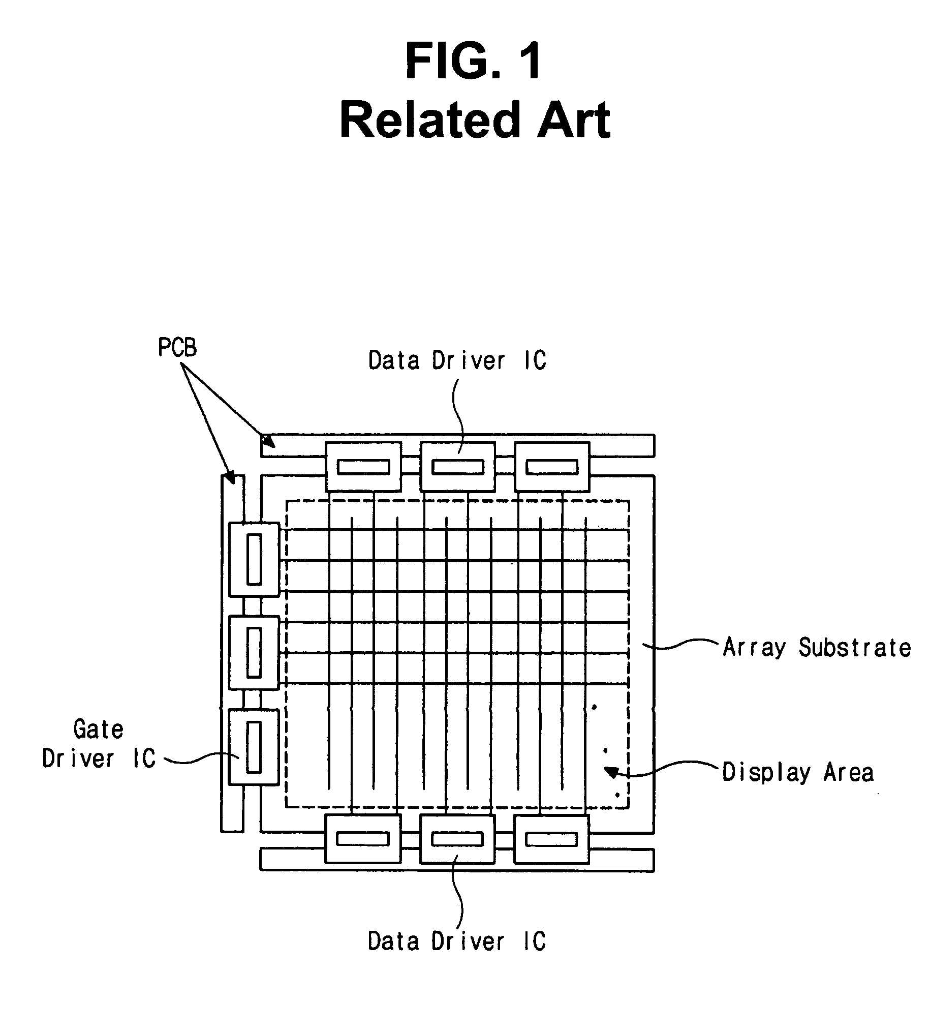
However, although the LCD device is better than the CRT in power consumption, the LCD device including amorphous silicon is very expensive.
Accordingly, the driver IC is very costly.
Accordingly, this decreases reliability and productivity of the LCD device.
Additionally, this raises the cost of the LCD device.
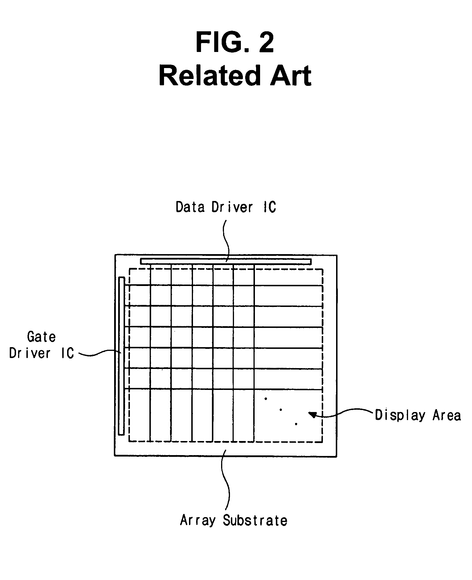
Since devices that include active layers made of amorphous silicon are expensive to fabricate, LCD devices that include polycrystalline silicon as active layers of the TFTs have been developed.
The leakage current causes residual images that lead to degradation of pixels of the LCD device.
However, since the LCD device includes storage capacitors, it is difficult to apply the DC voltage to the pixel TFTs.

Method used


Image

  • System and method for reducing off-current in thin film transistor of liquid crystal display device
  • System and method for reducing off-current in thin film transistor of liquid crystal display device
  • System and method for reducing off-current in thin film transistor of liquid crystal display device

Examples


Embodiment Construction

[0042]Reference will now be made in detail to the preferred embodiments of the present invention, examples of which are illustrated in the accompanying drawings.

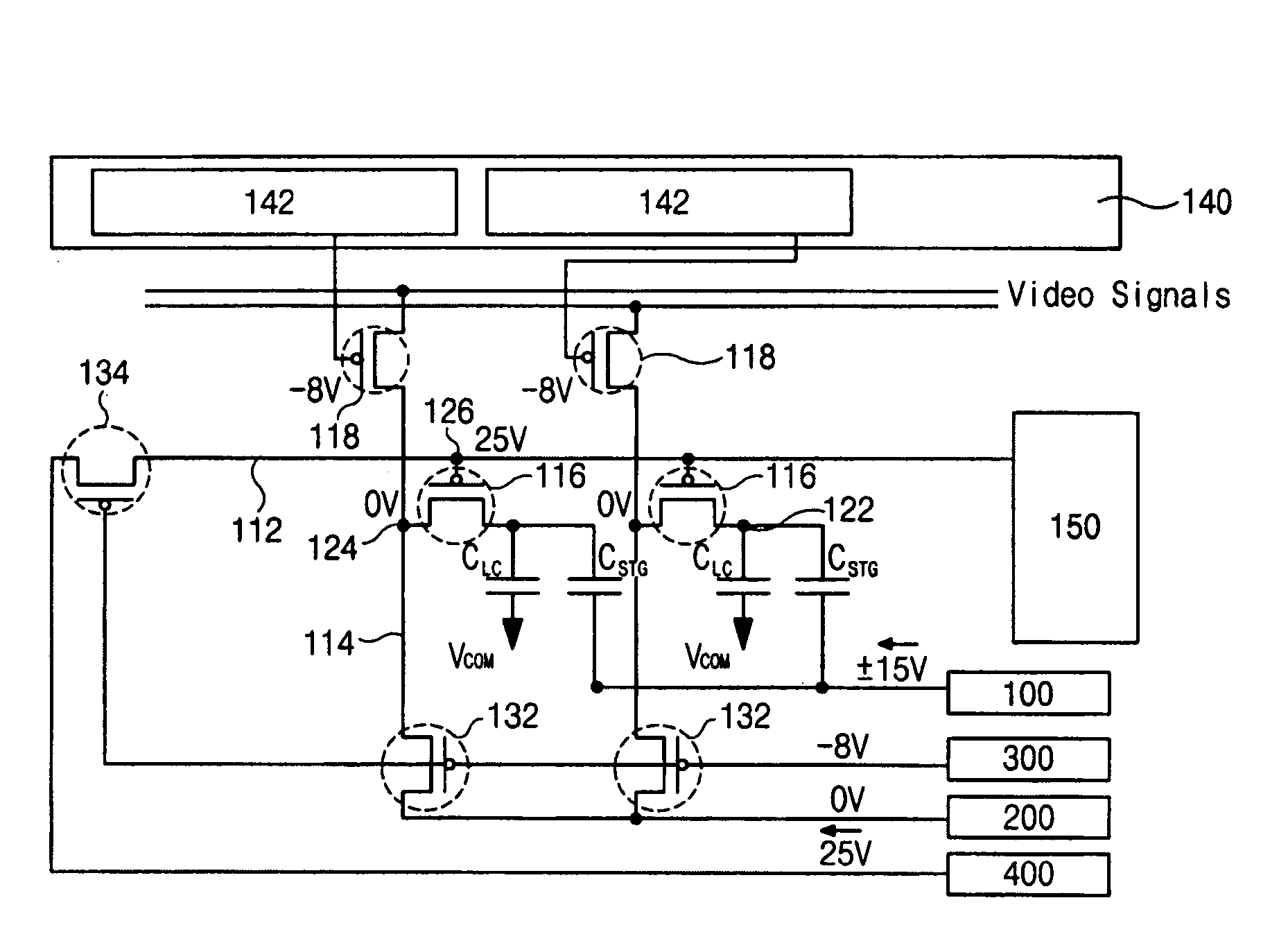
[0043]FIG. 6 is an exemplary schematic view of a liquid crystal display (LCD) device according to the present invention. In FIG. 6, a gate line 112 and a data line 114 cross each other to define a pixel region, wherein a pixel thin film transistor (TFT) 116 may be formed. A gate electrode of the pixel TFT 116 may be connected to the gate line 112 and a source electrode of the pixel TFT 116 may be connected to the data line 114. A liquid crystal (LC) capacitor CLC may be connected to a drain electrode of the pixel TFT 116 and a common electrode VCOM. One electrode of a storage capacitor CSTG may be also connected to the drain electrode of the pixel TFT 116, wherein the storage capacitor CSTG may be in parallel to the LC capacitor CLC. Accordingly, the storage capacitor CSTG and the LC capacitor CLC may form a first node 122. ...


PUM


Abstract

A system for reducing an OFF-current in a thin film transistor of a liquid crystal display device includes gate and data lines crossing each other, a pixel thin film transistor including gate, source and drain electrodes, the gate electrode connected to the gate line and the source electrode connected to the data line, a liquid crystal capacitor connected to the drain electrode of the pixel thin film transistor, a first switch thin film transistor connected to a first end of the data line, a second switch thin film transistor connected to a first end of the gate line, a first voltage source electrically connected to the drain electrode of the pixel thin film transistor, a second voltage source connected to a source electrode of the first switch thin film transistor, a third voltage source connected to gate electrodes of the first and second switch thin film transistors, and a fourth voltage source connected to a source electrode of the second switch thin film transistor.

Description

[0001]The present invention claims the benefit of Korean Patent Application No. 2002-76723 filed in Korea on Dec. 4, 2002, which is hereby incorporated by reference.BACKGROUND OF THE INVENTION[0002]1. Field of the Invention[0003]The present invention relates to a liquid crystal display device including a thin film transistor and more particularly, to a system and a method for reducing OFF-current in a thin film transistor of a liquid crystal display device.[0004]2. Discussion of the Related Art[0005]Due to rapid development in information technology, display devices have to display large amounts of information. Although cathode ray tube (CRT) devices have been commonly used as display devices, flat panel display devices have been developed that are thin, light weight, and low in power consumption. Among these, liquid crystal display (LCD) devices have been used in notebook computers and desktop monitors because of their superior image resolution, color image display, and display ima...

Claims


Application Information

Patent Timeline
Patent Type & Authority Patents(United States)
IPC IPC(8): G09G3/36
CPCG09G3/3655G09G3/3677G09G3/3688G09G2300/0876G09G2320/0257G09G3/36
Inventor PARK, JAE-DEOKKIM, BYEONG-KOOKIM, KEE-JONG
Owner LG DISPLAY CO LTD
Learn More