Method of manufacturing an IC coil mounted in an information carrier

a technology of information carrier and ic coil, which is applied in the field of ic elements, can solve the problems of reducing the cost of manufacturing the desired information carrier, and increasing the range or distance of communication with the reader/writer

Inactive Publication Date: 2006-10-31
HITACHT MAXELL LTD
View PDF30 Cites 38 Cited by
  • Summary
  • Abstract
  • Description
  • Claims
  • Application Information

AI Technical Summary

Benefits of technology

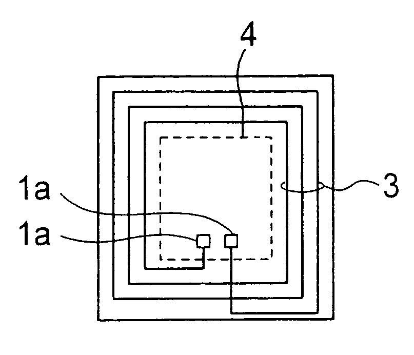
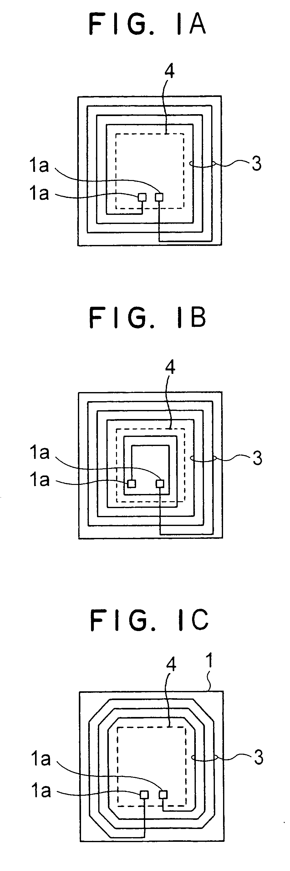
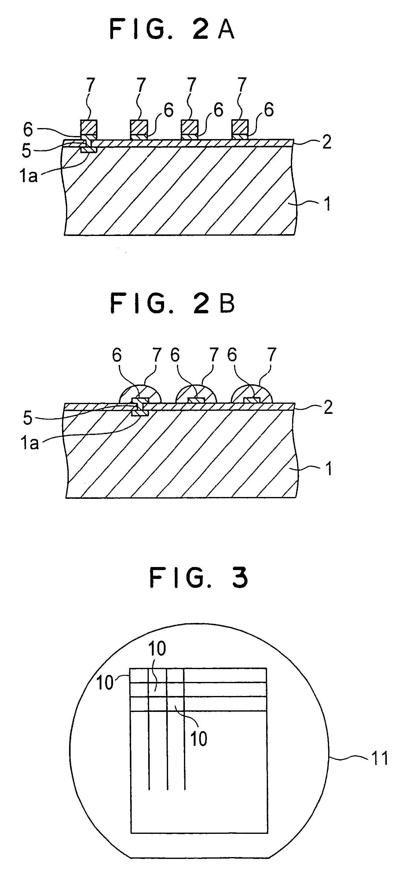
[0011]Since the metal-plated layer has an electric resistance value smaller than the metal-sputtered layer or alternatively the metal-evaporated layer, loss of the electromagnetic energy can be diminished by implementing the electric conductor of the coil in a multilayer structure composed of the metal-sputtered layer or alternatively the metal-evaporated layer and the metal-plated layer when compared with the coil conductor constituted solely by the metal-sputtered layer or alternatively the metal-evaporated layer, whereby the distance or range for communication with the reader / writer can be increased.<IC Element Manufacturing Method>
[0014]As is apparent from the above, by forming the required electric conductive pattern inclusive of the coil on the finished wafer to thereby obtain the concerned IC element by scribing the finished wafer, the IC element formed integrally with the coil can be manufactured with high efficiency when compared with the case where each of the individual IC elements are formed with a coil, whereby the manufacturing cost can be reduced. Furthermore, it is possible to implement the coils of a uniform thickness with high precision for all the IC elements formed on the wafer, whereby variance or dispersion of the communication characteristics can be suppressed.
[0017]By disposing the IC element on the substrate at the center portion as viewed in the planar direction of the substrate as mentioned above, the center of the coil formed integrally with the IC element and that of the antenna coil for the reader / writer can be easily aligned to each other. Thus, the coefficient of the electromagnetic coupling between both coils can be increased, whereby the electric power supply to the information carrier from the reader / writer as well as the signal transmission / reception between the reader / writer and the information carrier can be carried out with enhanced reliability. In particular, when the substrate which constitutes the information carrier is shaped in a square shape, a regular-polygonal shape or the like which exhibits no or less directivity relative to the reader / writer, the center of the coil formed integrally on the IC element can be aligned more easily with that of the antenna coil provided for the reader / writer, which allows the information carrier to be handled more facilitatively.
[0020]As is apparent from the above, the strip lamination in which the required IC elements (or alternatively the IC elements and the coils) are embedded is manufactured, whereon the concerned or desired information carriers are formed by punching the strip lamination. Thus, the identical information carriers can be manufactured with high efficiency, whereby the cost involved in manufacturing the desired information carriers can be reduced.

Problems solved by technology

In this conjunction, it is however noted that when the antenna coil is formed integrally on the IC element, not only the winding diameter and the conductor width of the coil become smaller when compared with the case where the antenna coil composed of the winding is carried on the substrate, but also the number of turns of the coil is naturally limited, making it difficult to increase the range or distance for communication with the reader / writer or rendering it even impossible to ensure the communication range.

Method used


Image

  • Method of manufacturing an IC coil mounted in an information carrier
  • Method of manufacturing an IC coil mounted in an information carrier
  • Method of manufacturing an IC coil mounted in an information carrier

Examples


second embodiment

[0070]Referring to FIG. 11, an information carrier 20b includes a substrate 21 constituted by a top member 22, an intermediate member 23 and a bottom member 24 and features disposition of a booster coil 28 in a concentric circular array around the IC element 1. In the figure, reference numeral 29 denotes a recess for accommodating therein the booster coil 28, wherein the recess is formed in a ring-like shape around a through-hole 27 of the intermediate member 23. In the other respects, the structure of the information carrier according to the second exemplary embodiment is identical with that of the information carrier 20a according to the first exemplary embodiment. Accordingly, repeated description thereof is omitted. The information carrier 20b according to the instant exemplary embodiment presents similar advantageous effects as those of the information carrier 20a according to the first exemplary embodiment. In addition, by virtue of the concentric circular disposition of the ...

first embodiment

[0083]A first example of the information carrier manufacturing method according to the present invention is destined for manufacturing the information carrier 20a according to the first exemplary embodiment by using one sheet of strip material 41 shown in FIG. 18 and two sheets of strip materials 45 shown in FIG. 22. At first, one of the strip materials 45 is bonded to one surface of the strip material 41 with the adhesive layer 25 being interposed therebetween to thereby obtain a unitary bonded strip composed of the strip materials 41 and 45 having spaces within which the IC elements 1 can be accommodated, respectively. Subsequently, the IC elements 1 are positioned to be placed within the spaces mentioned above, respectively, whereon the IC elements 1 are bonded to the strip material 45 by using the adhesive layers 25, respectively. In succession, the other strip material 45 is bonded to the other surface of the strip material 41 with the adhesive layer 25 interposed therebetween ...


PUM


Abstract

An information carrier in which an IC element formed integrally with a coil is mounted and which has an extended communication range and a method of manufacturing the same and a structure of the IC element appropriately suited for this sort of information carrier and a method of manufacturing the same. In the IC element, a conductor constituting the coil 3 is implemented in a multilayer structure including a metal-sputtered layer or alternatively a metal-evaporated layer 6 and a metal-plated layer 7. In the method of manufacturing the IC element, a precision electroforming method is employed as a means for forming the metal-plated layer 7. The information carrier is implemented in such a structure in which the IC element 1 is disposed at a center portion in a planar direction of a substrate 21. In a method of manufacturing the information carrier, strip material or materials 41 to 45 a given one of which has mounted thereon desired parts inclusive of the IC elements are manufactured, whereon desired information carriers 20a, . . . , 20h are formed by punching the strip material(s).

Description

[0001]This application is a Divisional of application Ser. No. 09 / 914,077 filed on Aug. 23, 2001 now abandoned, and for which priority is claimed under 35 U.S.C. § 120. application Ser. No. 09 / 914,077 is the national phase of PCT International Application No. PCT / JP00 / 01029 filed on Feb. 23, 2000, under 35 U.S.C. § 371. The entire contents of each of the above-identified applications are hereby incorporated by reference. This application also claims priority of Application Nos. 11-046545 and 11-059753 filed in Japan on Feb. 24, 1999, and Mar. 8, 1999, respectively, under 35 U.S.C. § 119.BACKGROUND OF THE INVENTION[0002]1. Field of the Invention[0003]The present invention relates to AN IC element formed integrally with a coil on a chip, a method of manufacturing the IC element, an information carrier incorporating the IC element and a method of manufacturing the information carrier.[0004]2. Description of Related Art[0005]Heretofore, such a contactless type information carrier has be...

Claims


Application Information

Patent Timeline
Patent Type & Authority Patents(United States)
IPC IPC(8): H01L21/20G06K19/077H01L23/498H01L23/522
CPCG06K19/07749G06K19/07775G06K19/07779H01L23/49855H01L23/5227H01L2924/0002H01L2924/00H01L25/00
Inventor KAWAMURA, SATOSHISHIMIZU, SHIN
Owner HITACHT MAXELL LTD
Why Eureka
Try Eureka