Testing device and testing method of a semiconductor device

a testing device and semiconductor technology, applied in the direction of measurement devices, semiconductor/solid-state device testing/measurement, instruments, etc., can solve the problems of difficult to perform a characteristic test on the back terminal of a semiconductor device such as the pop, and difficult to perform a temperature control

Inactive Publication Date: 2006-10-31
SOCIONEXT INC
View PDF8 Cites 26 Cited by
  • Summary
  • Abstract
  • Description
  • Claims
  • Application Information

AI Technical Summary

Benefits of technology

[0043]According to the present invention, the semiconductor device is mounted on the support board with the back surface, which is opposite to the electrodes of the semiconductor device, facing downward, and is pressed onto the contactor in a state where the back surface is supported by the press head. The semiconductor device pressed by the contactor is selected by placing one of the semiconductor devices held by the support board by horizontally moving the stage. Accordingly, only a vertically moving mechanism is provided to the press head, which can make the press head in a simple structure. Thus, the heater or the cooling unit for temperature control can be provided to the press head so as to support the back surface of the semiconductor device, which is close to a heat radiator plate, by the press head, thereby performing a temperature control of the semiconductor device efficiently.

Problems solved by technology

Here, in the test method of A), it is difficult to perform a temperature control by cooling or heating the press head since the conveyance / press head moves in a wide range.
Additionally, it is very difficult to perform a characteristic test on back terminals of a semiconductor device such as the PoP.
Additionally, in the method of B), it is difficult to perform a temperature control and a characteristic test on the back terminals, like the above-mentioned method A), since the back surface of the semiconductor device is covered due to the semiconductor device being fixed to the stage in a state where the semiconductor device is reversed and accommodated in an arranging plate with the external connection terminals facing upward or in a state where it is applied onto a tacking tape.
Especially, with respect to the temperature control, since a temperature characteristic differs from semiconductor devices, a method (refer to Patent Document 3) of detecting a temperature of a part of the stage and performing a temperature control by cooling or heating a whole surface of the stage by feeding back a result of the temperature detection cannot control the semiconductor device at a desired temperature.
1) A measurement test by selecting an arbitrary semiconductor device cannot be performed since the tray accommodating the semiconductor devices in an aligned manner is sequentially moved.
3) A temperature control on a top side of a chip mounted inside cannot be performed since the semiconductor device is heated or cooled for the purpose of performing a test of a flat package, which provides a temperature control from a bottom surface of the package.
4) A temperature control of a plurality of semiconductor devices cannot be performed since a measurement test by selecting a plurality of arbitrary semiconductor devices cannot be performed.
On the other hand, in the characteristic test shown in FIG. 1, it is difficult to perform a temperature control such as cooling or heating the semiconductor devices 2 being tested since the press / suction head 5 moves in a wide range.
For example, it is difficult to provide to the press / suction head 5 a liquid cooling unit, heat releasing fins and a blower for air cooling or a heater for heating and a temperature sensor.
Additionally, in the characteristic test using the press / suction head 5 moving in a wide range, it is very difficult to perform a characteristic test by making an electrical contact to terminals of a semiconductor device such as the above-mentioned PoP that has external connection terminals on a back surface thereof.
For example, it is difficult to provide to the above-mentioned press / suction head 5 contact pieces as a contactor and pats and wiring for electric connection.
On the other hand, in the characteristic test method shown in FIG. 2, it is difficult to perform a temperature control such as cooling or heating since the back surface of the semiconductor device 12 is covered by the stage 13.
Thus, a heat resistance of the heat conducting path is large, and it is difficult to perform a temperature control.
Accordingly, when performing a characteristic test of semiconductor devices having different temperature characteristics, a temperature control of specific positions may be performed, but it is difficult to perform a characteristic test while controlling the temperatures of all the semiconductor devices to fall within a desired temperature range.
Thus, it is difficult to perform accurate positioning between the semiconductor devices 12 and the contactor 15.
Additionally, it is very difficult to perform a characteristic test by making an electrical contact with external connection terminals of a semiconductor device such as the PoP, which has the external connection terminals on the back surface thereof since the back surface of the semiconductor device 12 is covered by the conveyance tray 11.
Additionally, it is difficult to make an electrical contact to the terminals on the back surface of the semiconductor device 12 from the back side.

Method used


Image

  • Testing device and testing method of a semiconductor device
  • Testing device and testing method of a semiconductor device
  • Testing device and testing method of a semiconductor device

Examples


first embodiment

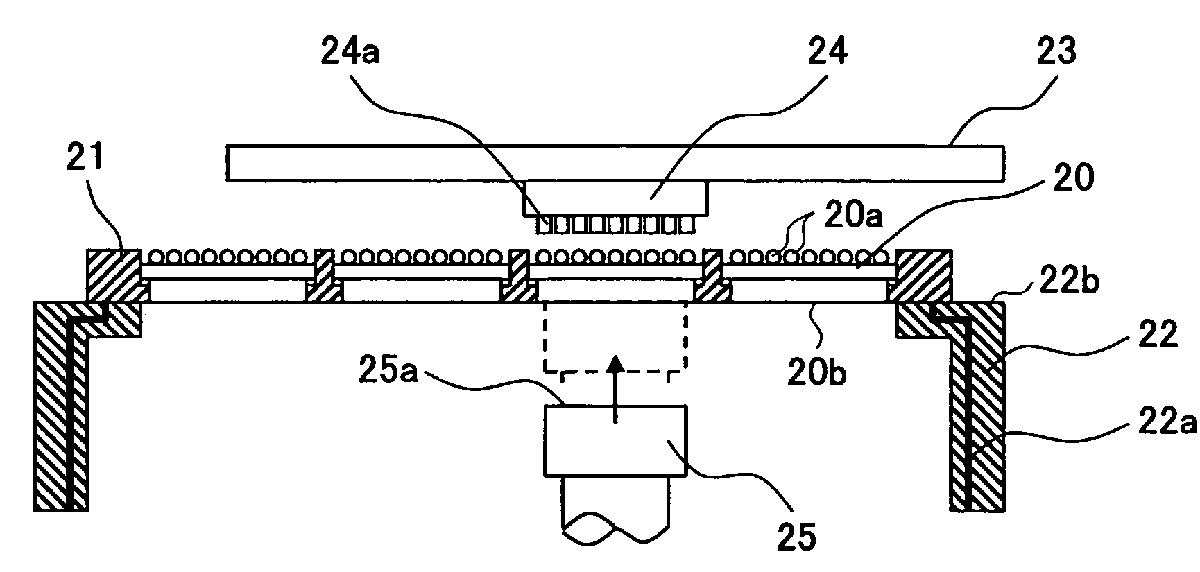
[0078]The testing method according to the present invention is performed by using a testing device that comprises, as shown in FIG. 7, a support board 21 on which a plurality of semiconductor devices 20 to be tested in an aligned state and a stage 22 that is formed in an annular shape to support a peripheral portion of the support board 21.

[0079]The support board 21 is made of a metal material such as aluminum or stainless steel or a resin material such as plastics. The support board 21 is provided with recessed portions 21a for accommodating the semiconductor devices 20 in an aligned state in an X direction and a Y direction. Each of the recessed portions 21a has a configuration substantially the same as the outer configuration of each of the semiconductor devices 20 and extends through the support board 21 so as to accommodate one of the semiconductor devices 20. Each of the recessed portions 21a has a step portion on an inner surface thereof so that each of the semiconductor devi...

third embodiment

[0146]A description will now be given, with reference to FIG. 28 and FIG. 29, of a testing device and a testing method of a semiconductor device according to the present invention. FIG. 28 shows a testing device and testing method for performing a characteristic test of the semiconductor device 20, which is provided with external connection terminals on the back surface 20b thereof.

[0147]As shown in FIG. 28, a contact piece 25Eb is provided to the press surface 25Ea of the press head 25E. The contact piece 25Eb is brought into contact with the external connection terminal 20c formed on the back surface 20b of the semiconductor device 20. The contact piece 25Eb has a configuration to receive the external connection terminal 20c. That is, the contact piece 25Eb of the press head 24E contacts and presses the external connection terminal 20c of the semiconductor device 20, thereby, pressing the external connection terminal20c of the semiconductor device 20 onto the contactor 24.

[0148]As...

fourth embodiment

[0153]A description will now be given, with reference to FIG. 30 and FIG. 31, of a test device and a test method of a semiconductor device according to the present invention.

[0154]In the testing device of a semiconductor device according to the fourth embodiment of the present invention shown in FIG. 30, a plurality of contactor 24-1, 24-2 and 24-3 are provided to the test circuit board 23, and a plurality of press heads 25-1, 25-2 and 25-3 area provided correspondingly. According to the contactors 24-1, 24-2 and 24-3 and the corresponding press heads 25-1, 25-2 and 25-3, a contact can be made simultaneously to a plurality of semiconductor devices.

[0155]In the testing device having the above-mentioned structure, as shown in FIG. 31, an upward movement of each of the press heads is controlled individually so as to selectively move the plurality of press heads upward and selectively test the semiconductor devices.

[0156]In the example shown n FIG. 31, the press heads 25-1 and 25-3 are ...


PUM


Abstract

A testing device can perform a test on an arbitrary one of a plurality of semiconductor devices by pressing the semiconductor devices onto a contactor from a back side of the semiconductor device. A test circuit board has a contactor provided with contact pieces corresponding to external connection terminals of semiconductor devices to be tested. A support board is capable of mounting the semiconductor devices thereon in an aligned state. A stage supports the support board. A press head presses the semiconductor devices to be tested mounted on the support board so as to cause external connection terminals of the semiconductor devices to be tested to contact with the contact pieces of the contactor. The stage is movable to a position at which at least one of the semiconductor devices to be tested, which are mounted on the support board, faces the contactor.

Description

BACKGROUND OF THE INVENTION[0001]1. Field of the Invention[0002]The present invention relates to testing devices and methods of a semiconductor device and, more particularly to a testing device and method for performing a characteristic test of a semiconductor device while taking an electric conduction to the semiconductor device.[0003]2. Description of the Related Art[0004]In recent years, with increase in electric current and power consumption of a semiconductor integrated circuit device (hereinafter, referred to as a semiconductor device) such as an MPU (Micro Processing Unit) for high-end users or a CPU (Central Processing Unit) for personal computers. In an SiP (System in Package) which constitutes a system by accommodating a plurality of semiconductor devices in a single outer package (accommodation container), there is a PoP (Package on Package) which constitutes a single outer package by mounting other semiconductor devices on a back surface of one semiconductor device.[0005...

Claims


Application Information

Patent Timeline
Patent Type & Authority Patents(United States)
IPC IPC(8): G01R31/02
CPCG01R31/2887H01L22/00
Inventor TASHIRO, KAZUHIROITOU, YASUYUKIMARUYAMA, SHIGEYUKIARISAKA, YOSHIKAZU
Owner SOCIONEXT INC
Why Eureka
Try Eureka