Control of a flash unit in a digital camera

a digital camera and control technology, applied in the direction of instruments, television systems, television system scanning details, etc., can solve the problems of large bandwidth for serial and digital transfer of image information out of the sensor circuit, row-by-row processing, and complex sensor structure, etc., to achieve compact digital camera, improve image resolution, and reduce power consumption.

Active Publication Date: 2006-10-31
NOKIA TECHNOLOGLES OY
View PDF18 Cites 18 Cited by
  • Summary
  • Abstract
  • Description
  • Claims
  • Application Information

AI Technical Summary

Benefits of technology

[0020]It is the primary aim of the present invention to disclose a method for controlling the operation of a flash unit in connection with a digital image sensor which is to be processed row by row, column by column or another sub-area at a time and which uses a rolling electronic shutter or the like and thereby operates without a separate external shutter. It is a particular aim of the invention to avoid the above-presented problems which impair the image quality due to the disparity between the duration of the flash of the flash unit (light pulse) and the time required for processing the whole image area of the sensor.
[0026]The significant advantage is attained by the present invention that it minimizes the number of light flashes required for one image while it also ensures that the object to be imaged is illuminated as evenly as possible during the exposer (RI) of each sub-area of the sensor. The minimization of the number of light flashes is very important particularly in portable and / or other battery-operated devices in which the total power consumption of the flash unit should be kept as low as possible to save the capacity of the batteries and / or to minimize their size.
[0027]By using the method of the invention, a very high image quality is also achieved, thanks to the even exposer of the image area. Furthermore, in the case of a moving object to be imaged, the invention effectively prevents blurring of the image caused by the movement of the object, in a way to be described more fully hereinbelow.
[0030]Further, the invention can also be applied in the storage of so-called super resolution images. In super resolution images, several successive images in which the object is slightly transferred with respect to the image area are combined by means of image processing into a single new image. The resolution of the combined image is better than the pixel resolution of the original images.
[0031]The invention is preferably applied particularly in connection with CMOS image sensors, to produce a simple, compact digital camera with a low power consumption. Such a digital camera is suitable to be placed e.g. in a mobile station or in another corresponding portable personal device.

Problems solved by technology

However, this will result in a very complex structure of the sensor.
Furthermore, the transfer of image information in serial and digital form out of the sensor circuit should use a considerably large bandwidth.
However, the row-by-row processing has the drawback that the different rows of the matrix sensor are now exposed at slightly different times. FIG. 1 shows, in principle, the row-by-row processing of the image sensor and its effect on the exposure of the different rows of the sensor.
However, in a situation in which an electronic flash unit (flash unit) is used for illuminating the object during the imaging, considerable problems will be caused to the image quality by the exposure of the sensor rows at different times. The reason for this is that because of the short flash time specific to the flash unit, the illumination produced by the flash unit will significantly change the time when the whole image area of the sensor is exposed / processed.
Now, as the flash of the flash unit is considerably shorter than the processing of the whole image area, this will cause that different rows of the sensor will be exposed in significantly different ways when the flash unit is used, and therefor, the quality of the images taken with the flash unit is impaired.

Method used


Image

  • Control of a flash unit in a digital camera
  • Control of a flash unit in a digital camera
  • Control of a flash unit in a digital camera

Examples


Embodiment Construction

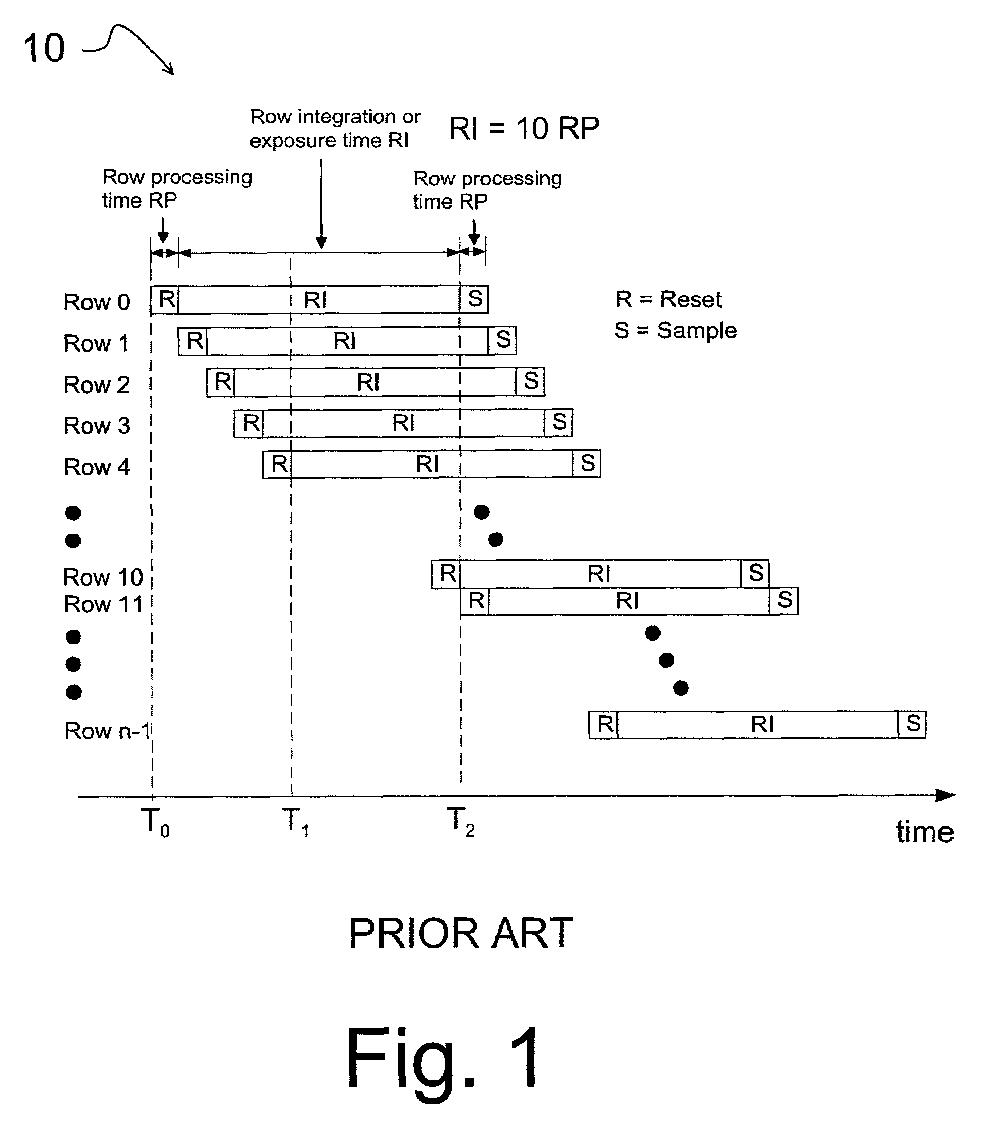
[0039]The operation of a rolling electronic shutter (10), shown in principle in FIG. 1, has already been discussed above in connection with the description of the prior art.

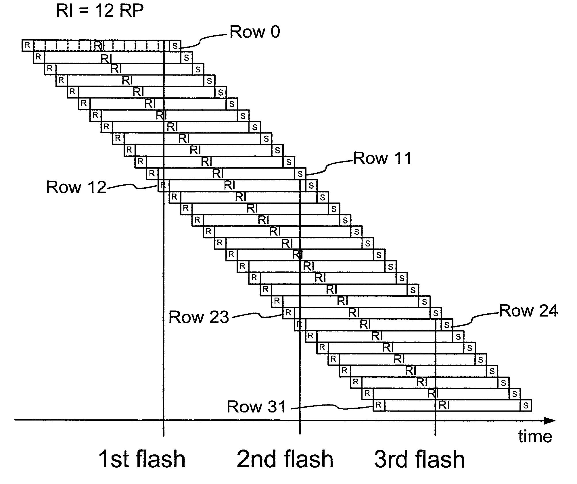
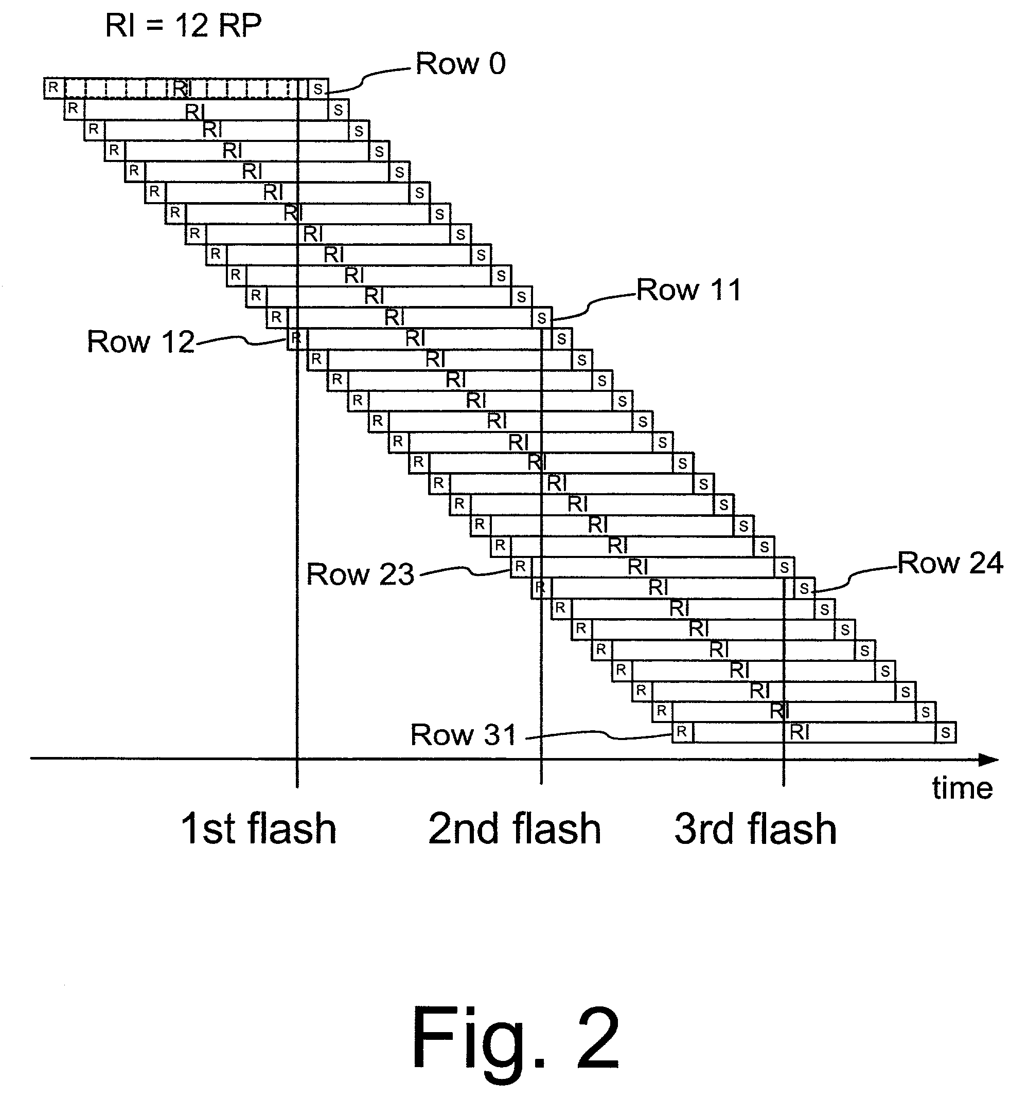
[0040]FIG. 2 shows, in principle, how the flashes of an electronic flash unit (hereafter flash unit) of the invention are timed in connection with a matrix sensor to be processed and exposed row by row according to Fig. 1 or in a way substantially corresponding to FIG. 1.

[0041]According to FIG. 2, the start of the integration or exposure time (RI) of each pixel row in the sensor is delayed from the start of the exposure time (RI) of the preceding row by the time of the reset function (R), i.e. by the row processing time (RP). For this reason, the exposure times of successive rows are shifted with respect to each other as shown in FIG. 2.

[0042]According to the invention, the flashes of the flash unit to be used for one image are timed in such a way that each single flash of the flash unit is triggered at a point o...


PUM


Abstract

The invention is based on a method for controlling a flash unit in connection with a digital image sensor without a mechanical shutter, wherein the exposure of the image sensor is performed in sub-areas, such as pixel rows or columns, or in another order, by using a rolling electronic shutter or the like. Thus, the exposure of said sub-areas of the image sensor takes place at least partly at different times. According to the invention, during the time of exposure of one image, i.e. substantially all the sub-areas of the image sensor, several discrete, successive flashes of the flash unit are used to achieve even exposure of the image area, which the flashes are timed in such a way that each single flash is triggered at a point of time which is common to the integration or exposure time of as many successive sub-areas of the image sensor as possible. According to the invention, the successive light flashes are also timed in such a way that one and only one flash of the flash unit occurs during the integration or exposure time of each single sub-area. By the present invention, the significant advantage is attained that the invention minimizes the number of light flashes required for one image while it also secures that each sub-area of the sensor to be exposed at a different time is illuminated as evenly as possible.

Description

CROSS-REFERENCE TO RELATED APPLICATIONS[0001]Priority is claimed from Finnish application 20011155 filed 1 Jun. 2001.FIELD OF THE INVENTION [0002]The invention relates to a method for controlling the operation of a flash unit in connection with an electronic image sensor operating without a separate external shutter.BACKGROUND OF THE INVENTION [0003]Digital image sensors based on semiconductor technology, such as matrix sensors based on charge coupled devices (CCD) and complementary metal oxide semiconductor (CMOS) technology, now make it possible to provide a large variety of devices with built-in imaging functions. Such image sensors are used e.g. in digital video and still cameras intended for consumers, as well as in various camera devices connected to computers, such as so-called network cameras. Thanks to their high degree of integration, compact size and low power consumption, particularly CMOS sensors are also very suitable for use in small-size portable devices, such as mob...

Claims


Application Information

Patent Timeline
Patent Type & Authority Patents(United States)
IPC IPC(8): H04N5/222G03B9/70H04N5/235
CPCH04N5/2354H04N5/3532H04N23/74H04N25/531
Inventor RANTANEN, HENRYYRJANAINEN, JUKKA
Owner NOKIA TECHNOLOGLES OY
Why Eureka
Try Eureka