Miniaturized contact spring

a contact spring and miniaturized technology, applied in the direction of coupling device connection, semiconductor/solid-state device details, instruments, etc., can solve the problems of reducing the height of the probe required for compliance, too long freestanding springs, and insufficient strength to hold backside, so as to minimize the adhesion of contact pad materials, improve yield strength and fatigue strength, and ensure the effect of quality

Inactive Publication Date: 2006-11-21
ADVANTEST SINGAPORE PTE LTD
View PDF25 Cites 15 Cited by
  • Summary
  • Abstract
  • Description
  • Claims
  • Application Information

AI Technical Summary

Benefits of technology

[0018]This invention provides a solution to increase the yield strength and fatigue strength of miniaturized contact springs, which can be fabricated in arrays with ultra-small pitches. It also discloses a solution to minimize adhesion of the contact pad materials to the spring tips upon repeated contacts without affecting the reliability of the miniaturized springs. In addition, the invention also presents a solution to fabricate the springs that allow passage of relatively higher current without significantly degrading their lifetime. Also, the invention provides a solution for fabricating robust springs for joining die-bonding terminals to corresponding input-output pads of a substrate comprising an inorganic or organic material for reliable package fabrication. The joining can be facilitated, for example, through the use of solder or conducting adhesives including anisotropically conducting adhesive films.

Problems solved by technology

The problem in this kind of springs is that they are too long.
However, at the dimensions needed to probe ICs with pad pitches below 150 μm the freestanding springs have insufficient strength to hold backside photo resist without significantly reducing the probe height required for compliance.
Any non-uniformity in the photo process also translates to non-uniform spring heights that cannot meet the uniformity requirements necessary to stay on the IC pads while testing.
The method described in application (WO 01 / 48870)) also has an additional problem in controlling lift height after plating.
Both of these stress conditions are difficult to control for the tolerances and spring lift uniformity needed to test ICs.
In addition, compressive springs are stronger than tensile springs and the spring with a compressive plated film loses lift height to the point that there is not enough compliance for it to still be a useful probe.
There is also a limit to how high a freestanding spring can be lifted prior to plating to compensate for this compression effect.
As a result, the process taught by this patent application does not meet the requirements for controlling uniformity of the lift height of arrays of springs required for IC testing.
As a result, the freestanding portion of the spring is mechanically weaker in the vicinity of the base region.
Because the bending moment is the highest in this region, upon application of a force to the spring tip during IC test, the springs fracture early and therefore can not meet the probe lifetime requirement needed in IC manufacturing lines.
The mask alignment and control of spring release process also pose serious problems resulting in uneven plating and a variation in lift uniformity.
Another major problem in this process arises from the high resistivity of the relatively thin release layer, as well as the stress metal film, through which the plating current flows.
As a result, this process does not produce arrays of springs with reasonably uniform and controlled properties, such as lift height that is essential for effective IC testing.
The miniaturized contact springs are subjected to a large number of contact operations during testing which subject the springs to various levels of stresses including cyclic stresses.
Also, in packages that use contact springs to join two components, such as chips and chip carriers, the springs are subjected to stresses during testing and operation.
However, we have observed that the miniaturized springs, such as those with a size of around 400 μm×60 μm×20 μm, start to fail, i.e. being plastically deformed and / or fractured, typically after 10,000 touchdowns, where the contact force exceeds about 1 gf.
A major reason of the failure is that the resulting alternating stresses exceed fatigue strength of the spring material.
Springs with larger cross-sections can withstand similar or larger force without failure because the resulting stresses are lower, but they limit the pitch at which springs can be built.
However, a higher contact force increases the stress developed in the body of the spring, particularly near the base region, and thus increases the probability of early spring failure during repeated touchdowns.
This also shortens the springs' lifetime.

Method used


Image

  • Miniaturized contact spring
  • Miniaturized contact spring
  • Miniaturized contact spring

Examples


Embodiment Construction

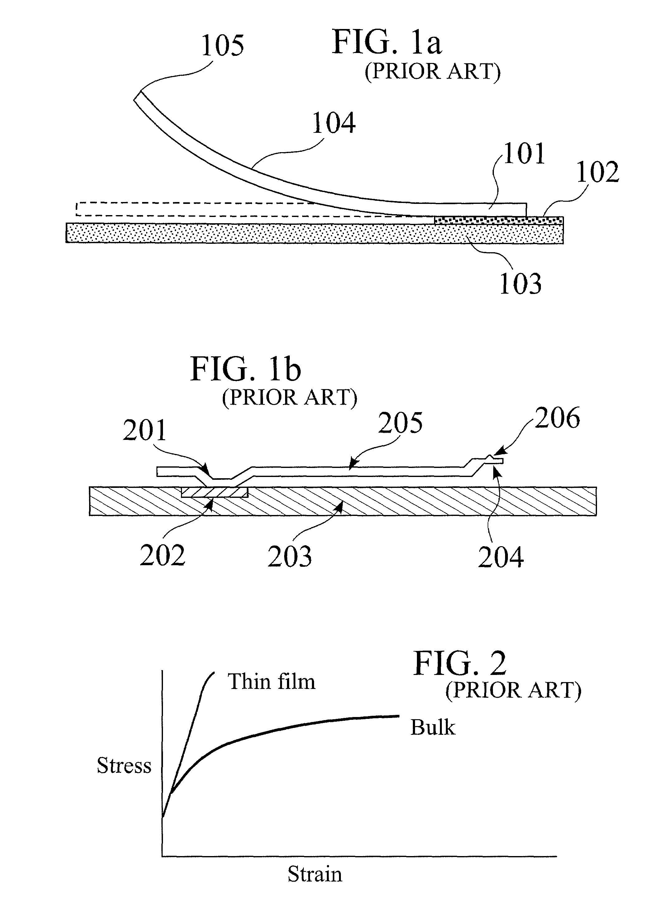
[0054]Miniaturized springs can be fabricated using thin film or discrete component fabrication technologies such as wire bonding. In general, for springs to perform satisfactorily in wide range of applications, the yield strength of the materials is required to be higher than the stresses applied to the springs during testing or burn-in, or in assembled packages. We have observed that many thin film stress metal springs are plastically deformed during testing because the spring material's yield strength is lower than the applied stress. A stress metal film typically comprises a strong core film composed of materials, such as molybdenum (Mo) or its alloys, tungsten (W) or its alloys, with additional overlying film coatings, such as nickel or nickel-cobalt (Ni—Co) alloy films. Some of these films are relatively thick, typically 4×10³ to 104 nm in thickness, which is required in order to increase the force that needs to be applied by the spring to the contacting surface for establishin...


PUM


Abstract

This invention provides a solution to increase the yield strength and fatigue strength of miniaturized springs, which can be fabricated in arrays with ultra-small pitches. It also discloses a solution to minimize adhesion of the contact pad materials to the spring tips upon repeated contacts without affecting the reliability of the miniaturized springs. In addition, the invention also presents a method to fabricate the springs that allow passage of relatively higher current without significantly degrading their lifetime.

Description

CROSS REFERENCE TO RELATED APPLICATION[0001]This application claims benefit of U.S. Provisional Patent Application Ser. No. 60 / 365,265 filed Mar. 19, 2002 now abandoned and is related U.S. patent application Ser. Nos. 09 / 979,551 filed May 26, 2000; Ser. No. 09 / 980,040 filed Jul. 28, 2000; Ser. No. 10 / 094,370 filed Mar. 8, 2002; Ser. No. 10 / 069,902 filed Nov. 21, 2002 and International Patent Application PCT / US02 / 26785 filed on Aug. 23, 2002, each of which of which is incorporated herein in its entirety by this reference thereto.BACKGROUND OF THE INVENTION[0002]1. Technical Field[0003]This invention relates generally to the highly miniaturized springs. More particularly, this invention relates to a family of miniaturized contact springs and a family of methods for increasing the yield strength and fatigue strength of these springs.[0004]2. Description of the Prior Art[0005]Miniaturized springs have been widely used as electrical contacts to contact pads or I / O terminals on integrated...

Claims


Application Information

Patent Timeline
Patent Type & Authority Patents(United States)
IPC IPC(8): H01R12/00H05K1/00B81B3/00G01R1/067G01R3/00H01L23/48H01R13/24H05K3/40H05K7/10
CPCB81B3/0072G01R3/00H01L21/4853H01L23/49811H01L24/72H05K7/1061B81B2201/018G01R1/06761H01L2924/01013H01L2924/01015H01L2924/01027H01L2924/01029H01L2924/0104H01L2924/01042H01L2924/01046H01L2924/01074H01L2924/01077H01L2924/01078H01L2924/01079H01L2924/01082H01L2924/04941H01L2924/09701H01L2924/14H01R9/091H01R12/57H01R12/718H01R13/24H01R13/2442H05K3/4092H01L2924/01005H01L2924/01006H01L2924/01019H01L2924/01023H01L2924/01024H01L2924/01033H01L2924/01044H01L2924/01045H01L2924/01047H01L2924/01076
Inventor LAHIRI, SYAMAL KUMARSWIATOWIEC, FRANKCHONG, FU CHIUNGMOK, SAMMYCHIEH, ERH-KONGMILTER, ROMAN L.HAEMER, JOSEPH M.LIN, CHANG-MINGCHEN, YI-HSINGDOAN, DAVID THANH
Owner ADVANTEST SINGAPORE PTE LTD
Why Eureka
Try Eureka