Semiconductor device having multiple-zone junction termination extension, and method for fabricating the same

a technology of junction termination and semiconductor device, which is applied in the direction of semiconductor device, basic electric element, electrical apparatus, etc., can solve the problems of difficult control of tapered mask formation, increased process cycle time and complexity, and inability to redistribute implanted dopant, etc., to achieve the effect of improving the performance of high-power semiconductor device and simplifying the fabrication of the devi

Active Publication Date: 2006-12-05
RENESSELAER POLYTECHNIC INST
View PDF5 Cites 24 Cited by
  • Summary
  • Abstract
  • Description
  • Claims
  • Application Information

AI Technical Summary

Benefits of technology

[0012]Some features of the invention arise from the realization that an effective, reproducible JTE implantation mask can be formed by etching of a mask layer to form a mask having steps of different thicknesses. The mask can be used during a single implant step to define a graded JTE. Features of the invention can be utilized to simplify the fabrication of, and improve the performance of, high-power semiconductor devices.

Problems solved by technology

Since SiC has very low dopant diffusivity, implanted dopant generally cannot be redistributed by annealing to modify its concentration distribution.
Multiple implantation steps can, however, increase process cycle time and complexity as well as fabrication cost.
Formation of a tapered mask, however, is difficult to control.
This approach also entails difficult process control, and over etching of the SiC is difficult to remedy.
Moreover, though commonly used, Reactive Ion Etching (RIE) can leave residual material damage resulting in increased leakage currents and diminished blocking performance.

Method used


Image

  • Semiconductor device having multiple-zone junction termination extension, and method for fabricating the same
  • Semiconductor device having multiple-zone junction termination extension, and method for fabricating the same
  • Semiconductor device having multiple-zone junction termination extension, and method for fabricating the same

Examples


Embodiment Construction

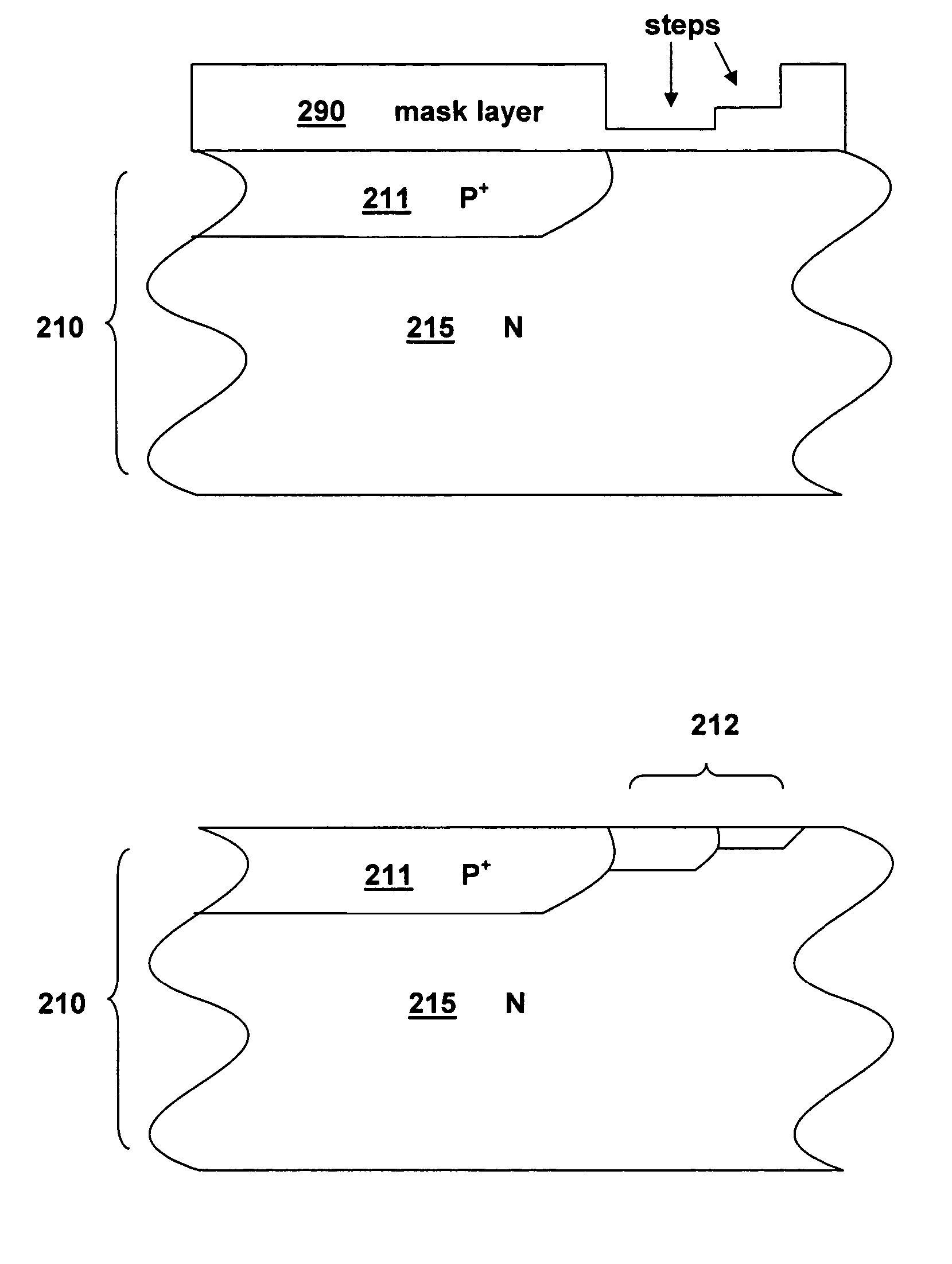
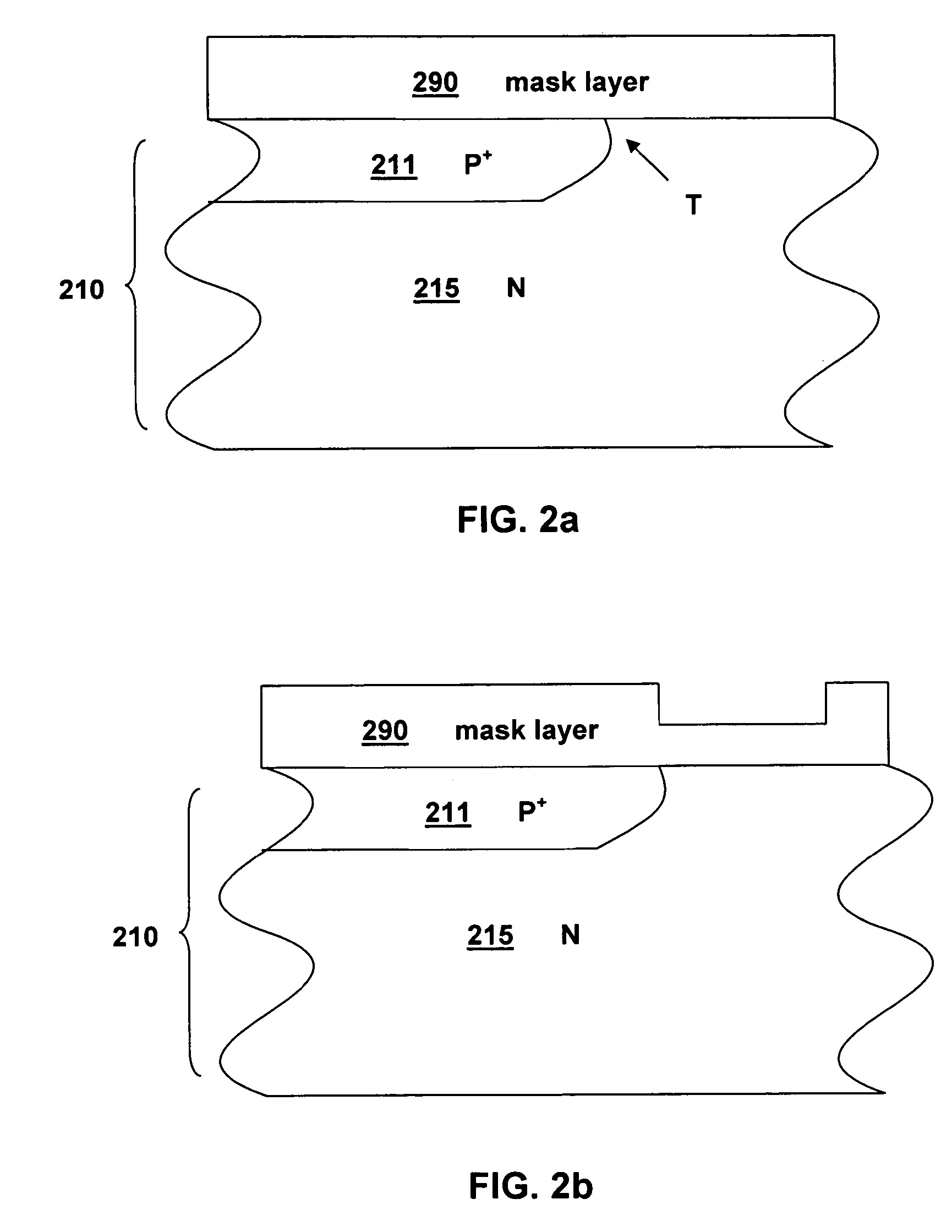
[0018]FIG. 1 is a flowchart of a method 100 for fabricating a semiconductor device, according to one embodiment of the invention. The method 100 includes providing a semiconductor layer 110 that has a pn junction, as defined, for example by the presence of dopant materials in the semiconductor layer 110. The pn junction has a termination at an interface of the semiconductor layer 110.

[0019]The method 100 also includes providing a mask layer 120 adjacent to the semiconductor layer, etching 130 the mask layer to form at least two laterally adjacent steps associated with different mask thicknesses and substantially planar step surfaces, implanting 10140 a dopant species through the mask layer into a portion of the semiconductor layer laterally adjacent to the junction termination, and annealing 150 the semiconductor layer to activate at least a portion of the implanted dopant species to form a graded termination extension for the junction termination.

[0020]The semiconductor layer 110 i...


PUM


Abstract

A semiconductor device includes a graded junction termination extension. A method for fabricating the device includes providing a semiconductor layer having a pn junction, providing a mask layer adjacent to the semiconductor layer, etching the mask layer to form at least two laterally adjacent steps associated with different mask thicknesses and substantially planar step surfaces, and implanting a dopant species through the mask layer into a portion of the semiconductor layer adjacent to the termination of the pn junction. The semiconductor layer is annealed to activate at least a portion of the implanted dopant species to form the graded junction termination extension.

Description

FEDERALLY SPONSORED RESEARCH[0001]This invention was made with Government support under DARPA Contract No. DAAD 19-02-1-0246, and NSF-ERC Contract No. EEC-9731677. The Government may have certain rights to this invention.BACKGROUND OF INVENTION[0002]1. Field of Invention[0003]The invention is related to semiconductor device structures and fabrication methods, and, more particularly, to high power devices and their fabrication.[0004]2. Discussion of Related Art[0005]The reverse-biased pn junctions in high-voltage semiconductor devices can exhibit 15 relatively low breakdown voltages due to electric field concentration at the termination of the pn junction. To mitigate this problem, some high-voltage devices include junction termination extensions (JTEs) that reduce the magnitude of field concentration. A JTE can extend laterally from a junction to spread a field over a larger area, and thus increase a voltage at which avalanche breakdown may occur.[0006]The laterally varying charge w...

Claims


Application Information

Patent Timeline
Patent Type & Authority Patents(United States)
IPC IPC(8): H01L21/22H01L21/332H01L21/425
CPCH01L21/0465H01L29/6606H01L21/2652
Inventor CHOW, TAT-SING PAULLOSEE, PETERBALACHANDRAN, SANTHOSH
Owner RENESSELAER POLYTECHNIC INST
Why Eureka
Try Eureka