Nitride semiconductor light emitting device and method for manufacturing the same

a light-emitting device and semiconductor technology, applied in the direction of semiconductor devices, basic electric elements, electrical appliances, etc., can solve the problems of difficult to provide a high brightness, electric current diffusivity, and inability to display the full range of natural colors, so as to reduce total current diffusivity, enhance brightness, and high brightness characteristics

Active Publication Date: 2006-12-26
SAMSUNG ELECTRONICS CO LTD
View PDF4 Cites 437 Cited by
  • Summary
  • Abstract
  • Description
  • Claims
  • Application Information

AI Technical Summary

Benefits of technology

[0011]Meanwhile, the nitride semiconductor light emitting device as shown in FIGS. 3a and 3b has an n-type electrode 3n or 37n formed on the n-type nitride semiconductor layer 33 such that like the conventional nitride semiconductor light emitting device shown in FIGS. 1a and 1b, some portions of an edge of the n-type nitride semiconductor layer 33 are exposed, and a p-type electrode 3p or 37p formed at the edge of the p-type nitride semiconductor layer 25 (or at the edge of the transparent electrode layer 36) opposite to the edge formed with the n-type electrode. In such a conventional nitride semiconductor light emitting device, there are provided advantageous effects that as indicated by the arrows in FIG. 3, the diffusion of the electric current can be generally carried out at the light emitting region, and that as shown in FIG. 5, the bonding wire does not block the light emitting region B after the package is produced.
[0012]However, a longer diagonal line between the edges formed with respective electrodes provides a longer distance through which the electric current passes, resulting in a non-uniform diffusion of the electric current, so that the difference between the brightness at the center of the light emitting region and that at the surrounding portions thereof increases. Particularly, since two electrodes are formed as points, there is provided a problem of reducing total current diffusivity.
[0013]Thus, there is a need to provide a nitride semiconductor light emitting device and a method of manufacturing the same, which is formed with the p-type electrode and the n-type electrode such that uniform light emission can occur at the entire light emitting region having the p-n junction, thereby realizing high brightness characteristics.SUMMARY OF THE INVENTION
[0014]Therefore, the present invention has been made in view of the above problems, and it is an object of the present invention to provide a nitride semiconductor light emitting device, which is formed with an electrode structure for providing uniform current diffusion, thereby enhancing brightness.
[0015]It is another object of the present invention to provides a method of manufacturing the nitride semiconductor light emitting device, which is formed with an electrode structure for providing uniform current diffusion, thereby enhancing brightness.
[0016]In accordance with an aspect of the present invention, the above and other objects can be accomplished by the provision of a nitride semiconductor light emitting device, comprising: a substrate having an approximately rectangular top surface; an n-type nitride semiconductor layer formed on the substrate and provided with an electrode region of a predetermined area adjacent to a center of one lateral side of the top surface of the substrate; an n-type electrode formed on the electrode region; an activation layer comprising an un-doped nitride semiconductor material and formed on the n-type nitride semiconductor layer such that the electrode region is exposed; a p-type nitride semiconductor layer formed on the activation layer; and a p-type electrode formed on the p-type nitride semiconductor layer, the p-type electrode having a bonding pad adjacent to a center of another lateral side opposite to the lateral side adjacent to the electrode region to have a predetermined space from the n-type electrode and having a band-shaped extension connected to the bonding pad to extend along a lateral side of the top surface of the p-type nitride semiconductor layer in opposite directions from a connected portion of the extension with the bonding pad.

Problems solved by technology

However, since the yellow-green LED has a lower brightness than that of the blue LED or the red LED and emits light having a wavelength of 565 nm or so which is not the wavelength of green required for the three primary colors, it is not possible to display the full range of natural colors.
However, in the electrode structure of the conventional nitride semiconductor light emitting device shown in FIG. 1, the p-type and the n-type electrodes are narrowly formed, thereby providing a low electric current diffusivity, and the p-n junction substantially contributing to the light emitting is formed around regions through which the electric current indicated by arrows in the drawings passes, thereby making it difficult to provide a high brightness.
Additionally, as indicated by the arrows in FIG. 1a, the distance of current diffusion varies, making it difficult to provide uniform current diffusion, thereby reducing the brightness.
Further, since the conventional nitride semiconductor light emitting device shown in FIG. 1 has the p-type electrode formed at the center of the upper surface of the nitride semiconductor light emitting device, when the package is formed using a bonding wire, the light emitting region is blocked by the bonding wire, as indicated by symbol A′ of FIG. 4, so that there is a problem that the brightness is further reduced after the package is manufactured.
However, there still exists the problem that since the p-type electrode 2p and 27p is disposed at the center of the light emitting region, the bonding wire blocks the light emitting region when manufacturing the package as shown in FIG. 4, thereby reducing the brightness.
Additionally, the method of manufacturing the nitride semiconductor light emitting device shown in FIGS. 2a and 2b should be accompanied by an etching process for exposing some portions of the periphery of the n-type semiconductor layer 23 in order to form the n-type electrode 2n or 27n thereon, and be formed with an n-type electrode having a narrow band shape on the exposed region around the periphery of the n-type semiconductor layer 23, thereby resulting in a complicated manufacturing process.
Further, the complicated and difficult process as described above increases manufacturing costs for the nitride semiconductor light emitting device.
Further, there is provided a problem of damaging the n-type electrode, during a scribing process for dividing a plurality of light emitting device formed on a wafer into separate chips.
However, a longer diagonal line between the edges formed with respective electrodes provides a longer distance through which the electric current passes, resulting in a non-uniform diffusion of the electric current, so that the difference between the brightness at the center of the light emitting region and that at the surrounding portions thereof increases.
Particularly, since two electrodes are formed as points, there is provided a problem of reducing total current diffusivity.

Method used


Image

  • Nitride semiconductor light emitting device and method for manufacturing the same
  • Nitride semiconductor light emitting device and method for manufacturing the same
  • Nitride semiconductor light emitting device and method for manufacturing the same

Examples


first embodiment

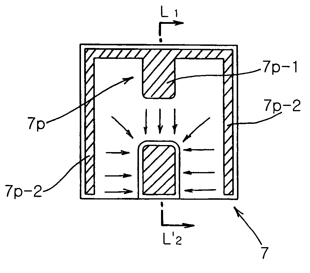
[0033]Referring to FIGS. 6a and 6c, a nitride semiconductor light emitting device 6 according to the present invention comprises: a substrate 61 having an approximately rectangular top surface; an n-type nitride semiconductor layer 63 formed on the substrate 61 and provided with an electrode region of a predetermined area adjacent to the center of one lateral side of the top surface of the substrate; an n-type electrode 67n or 6n formed on the n-type nitride semiconductor layer 63; an activation layer 64 comprising an un-doped nitride semiconductor material and formed on the n-type nitride semiconductor layer 63 such that the electrode region is exposed; a p-type nitride semiconductor layer 65 formed on the activation layer 64; and a p-type electrode 67p or 6p formed on the p-type nitride semiconductor layer 65. The p-type electrode 67p or 6p comprises a bonding pad 6p-1 adjacent to the center of a lateral side opposite to the lateral side adjacent to the electrode region to have a ...

second embodiment

[0038]The laminated structure of the nitride semiconductor light emitting device, which comprises the substrate 61, the buffer layer 62, the n-type nitride semiconductor layer 63, the activation layer 64, the p-type nitride layer 65 and the transparent layer 66, as described above, is also applied to the present invention, which will be described hereinafter.

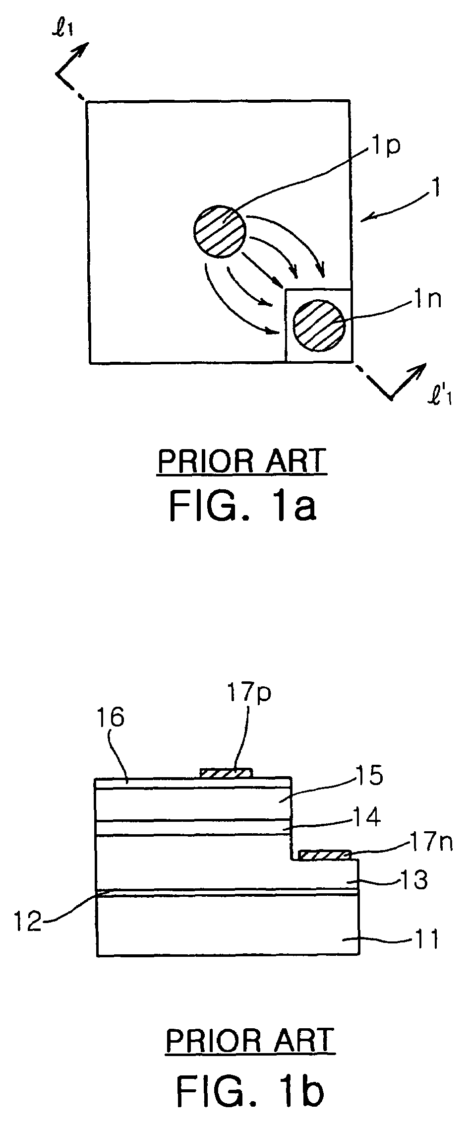
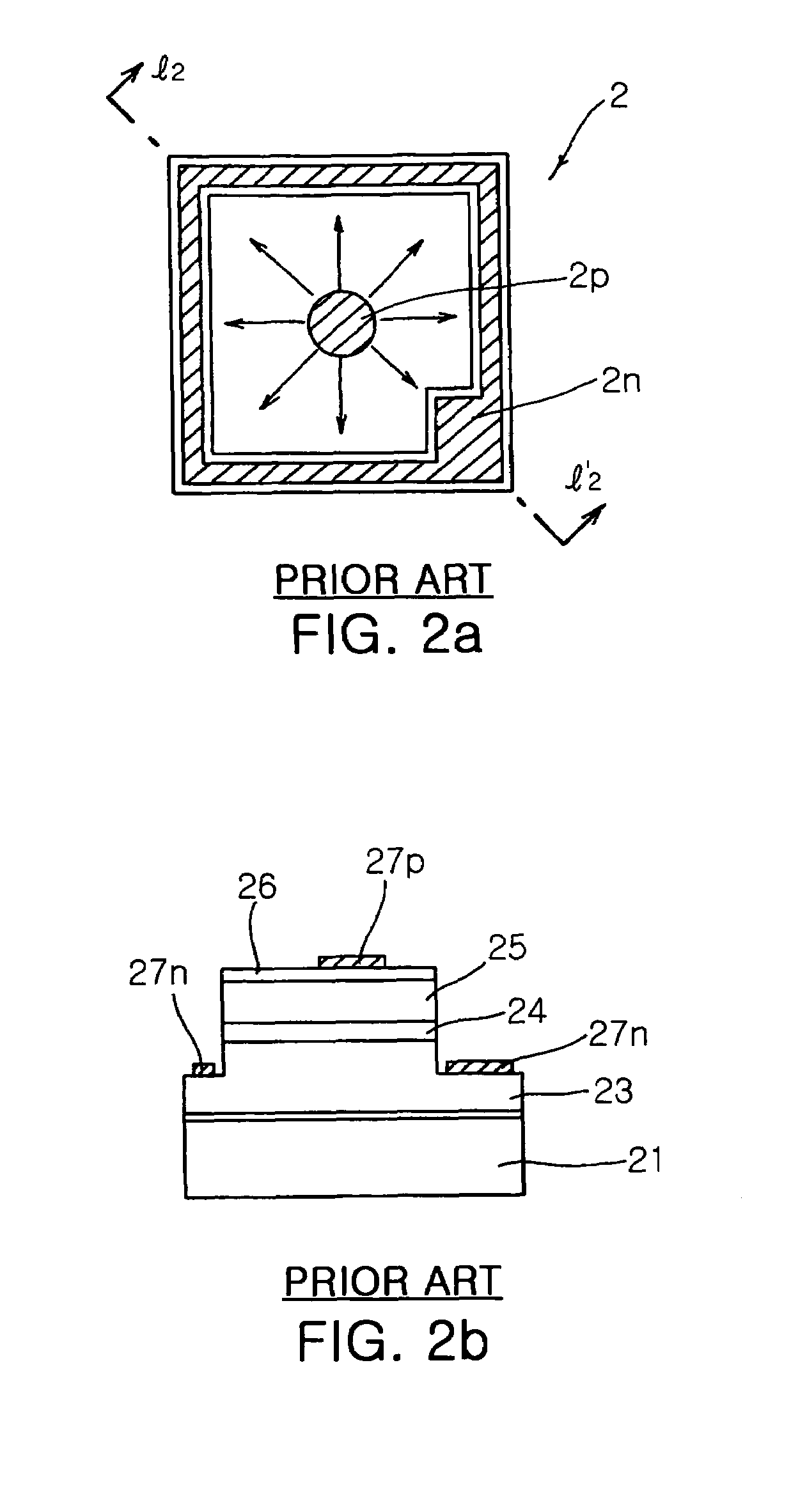
[0039]The present invention is primarily characterized by the structure of the p-type electrode 67p and the n-type electrode 67n for supplying power to the nitride semiconductor device. The enhanced structure of the electrodes in the present invention provides advantageous effects of enhancements in a current diffusivity in the nitride semiconductor device, in brightness characteristics and in driving voltage only by improving a metal patterning process, without greatly changing the manufacturing process and materials to be used for the nitride semiconductor light emitting device.

[0040]The nitride semiconductor light emitting de...


PUM


Abstract

A nitride semiconductor light emitting device includes a substrate, an n-type nitride semiconductor layer formed on the substrate and provided with an electrode region of a predetermined area adjacent to a center of one lateral side of the top surface of the substrate, an n-type electrode formed on the electrode region, an activation layer, a p-type nitride semiconductor layer, and a p-type electrode which has a bonding pad adjacent to a center of another lateral side opposite to the lateral side adjacent to the electrode region to have a predetermined space from the n-type electrode and a band-shaped extension connected to the bonding pad to extend along a lateral side of the top surface of the p-type nitride semiconductor layer in opposite directions from a connected portion of the extension with the bonding pad.

Description

BACKGROUND OF THE INVENTION[0001]1. Field of the Invention[0002]The present invention relates to a nitride semiconductor light emitting device, and more particularly to a nitride semiconductor light emitting device and a method of manufacturing the same, which can provide an improved electrode structure for the nitride semiconductor light emitting device to have uniform current diffusion and an increased current diffusion efficiency, thereby providing an enhanced brightness and driving voltage characteristics, and which can prevent a bonding wire from blocking a light emitting region when manufacturing a package, thereby preventing reduction in brightness after manufacturing the package.[0003]2. Description of the Related Art[0004]Recently, a light emitting device (LED) display board developed as a new transmission media for images or information has been advanced to a level of displaying a moving image, such as various CF images, graphic images, video display, etc., starting from i...

Claims


Application Information

Patent Timeline
Patent Type & Authority Patents(United States)
IPC IPC(8): H01L33/00H01L33/38
CPCH01L33/38H01L33/20H01L2933/0016H01L2224/48237H01L2224/48091H01L2224/49107H01L2924/181H01L2924/00014H01L2924/00012
Inventor HAN, YOUNG SUKKIM, SUNG WOOKYOON, SUK KIL
Owner SAMSUNG ELECTRONICS CO LTD
Why Eureka
Try Eureka