Input/output block with programmable hysteresis

a programmable hysteresis and input/output block technology, applied in the field of input/output blocks, can solve the problems of false output, low input swing, sensitive to noise,

Active Publication Date: 2006-12-26
STMICROELECTRONICS PVT LTD
View PDF7 Cites 11 Cited by
  • Summary
  • Abstract
  • Description
  • Claims
  • Application Information

AI Technical Summary

Problems solved by technology

High-speed switching circuits, where the switching speed is very high and input swing is very low are especially sensitive to noise.
These type of IOBs do not provide any hysteresis option and hence a small amount of noise in the inputs can result in a false output.
Further, though the hysteresis voltage can be changed by varying the reference voltages Vin1 and Vin2, this is not practically feasible since the sizes of the transistors are fixed in a circuit Therefore this circuit does not provide the flexibility to support different technologies.

Method used


Image

  • Input/output block with programmable hysteresis
  • Input/output block with programmable hysteresis
  • Input/output block with programmable hysteresis

Examples


Embodiment Construction

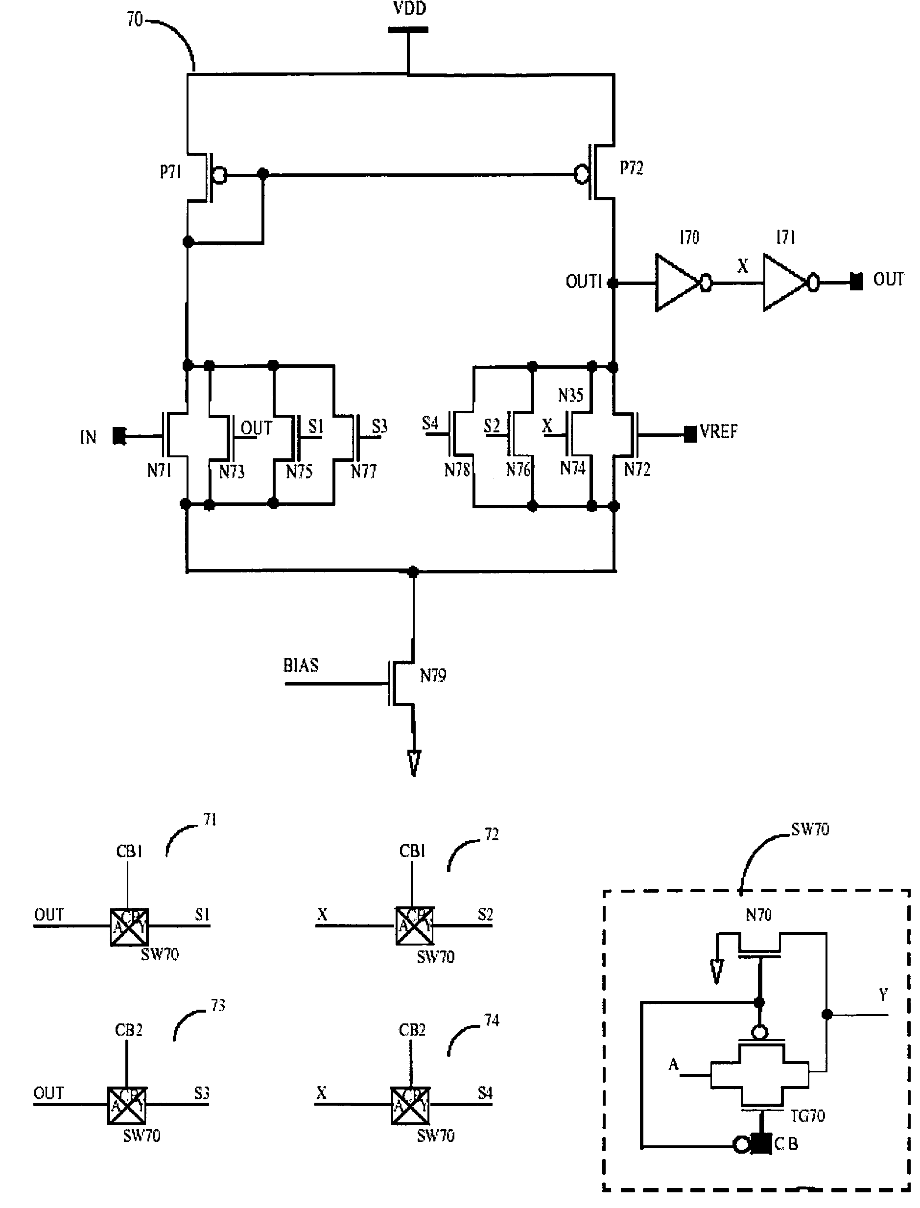
[0035]FIG. 5 shows a basic IOB in accordance with an embodiment of the present invention. The IOB has an NMOS differential input receiver comprising block 57 that is a load, and block 58 which is a current sink circuit. The load 57 is coupled to the current sink 58 through input transistors N51 and N52. Transistor N51 is controlled by input IN1 while transistor N52 is controlled by input IN2. For differential standards, IN1 and IN2 are differential inputs while for single ended standards IN2 is a reference voltage. Each input transistor N51, N52 has multiple transistors (only N53, N54, N55 and N56 are shown here) coupled in parallel with it as shown in the figure. Each transistor is of a predefined size to control the resistance offered by both the branches of input transistors. The transistors N53 and N54 are controlled by S1 and S3 while N54 and N56 are controlled by S2 and S4 respectively. The control signals S1, S2, S3 and S4 are generated by configuration bits and some feedback...


PUM


Abstract

An Input Output Block (IOB) provides programmable hysteresis to support multiple IO standards including a differential amplifier having one input coupled to an input signal and its second input coupled to a complementary input signal in the case of differential signalling, or to a reference voltage for the case of single-ended signalling, a pair of series coupled digital inverters coupled to one output of said differential amplifier, one or more transistors coupled in parallel with each input transistor of the differential amplifier, each transistor of each parallel coupled set being of a different size relative to the corresponding input transistor, the control terminal of each parallel coupled transistor in each set being coupled to the output of one of said series coupled inverters such that positive feedback is provided directly or indirectly through a selection switch, and hysteresis control bits that symmetrically enable or disable each said selection switch to provide a programmable level of hysteresis that is determined by the combination of selection switches that are enabled and the relative sizes of the corresponding parallel coupled transistors.

Description

RELATED APPLICATION[0001]The present application claims priority of Indian Patent Application No. 1430 / Del / 2003 filed Nov. 18, 2003.FIELD OF THE INVENTION[0002]This invention relates to Input / Output Blocks (IOBs) in integrated circuits. More particularly, the invention relates to IOBs with programmable hysteresis to support multiple IO standards for providing optimum noise margins.BACKGROUND OF THE INVENTION[0003]Hysteresis is an effective technique for enhancing the noise immunity of a logic circuit. High-speed switching circuits, where the switching speed is very high and input swing is very low are especially sensitive to noise. In such applications a precisely defined hysteresis voltage plays an important role in minimizing the effect of glitch signals. Different technologies supports different voltages i.e. the operating voltages and definition of the lower limit of threshold high (VIHmin) and upper limit of low (VILmax) level voltage varies with the technology used.[0004]FIG. ...

Claims


Application Information

Patent Timeline
Patent Type & Authority Patents(United States)
IPC IPC(8): H03K3/356H03K3/3565
CPCH03K3/3565
Inventor SHARMA, MANOJ KUMARKAUSHIK, RAJESH
Owner STMICROELECTRONICS PVT LTD
Why Eureka
Try Eureka