
Universal padset concept for high-frequency probing

Inactive Publication Date: 2007-01-02
SEIKO EPSON CORP
View PDF12 Cites 16 Cited by
  • Summary
  • Abstract
  • Description
  • Claims
  • Application Information

AI Technical Summary

Benefits of technology

[0025]It is an object of the present invention to minimize the number of additional test pad sets required for open-circuit and short-circuit test layouts, regardless of how the size of different DUTs vary.SUMMARY OF THE INVENTION
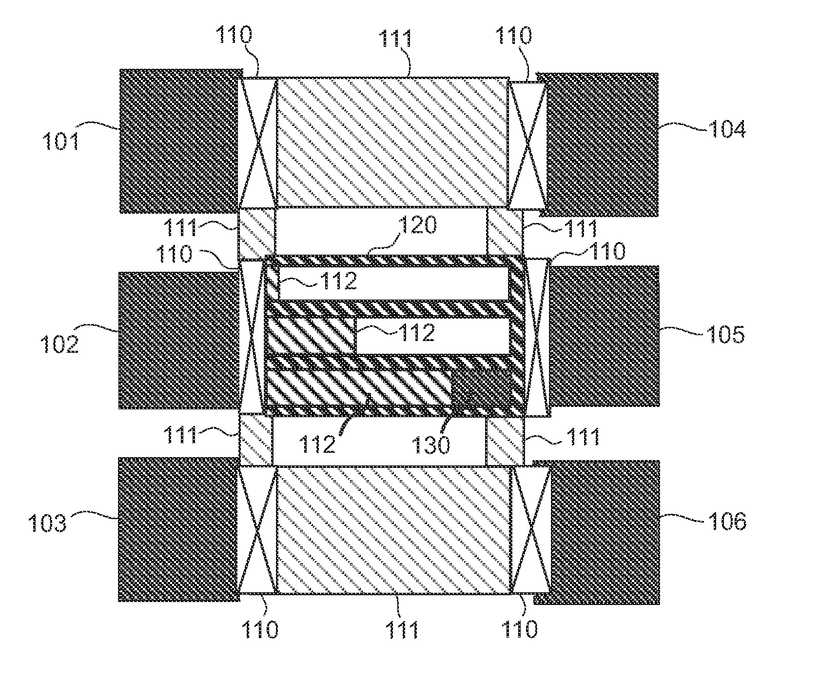
[0026]The present invention seeks to reduce the number of test pad sets and VNA calibrations sequences required to de-embed the loading effects of pads and probes for a large number of test devices, i.e. DUTs. This is accomplished by constructing multiple signal routing patterns suitable for coupling to the input / output nodes of multiple DUTs, but the multiple routing patterns all originate from a pre-set number of test pads sets. Generally, each test pad set includes three pads per test probe, i.e. each probe includes pins for contacting a signal line and two surrounding ground lines in a GSG format. Since the pad locations and the wiring routing pattern from the test pad sets is the same for the multiple test devices, DUTs, the loading effects of each test pad set and test probe is the same for all of the multiple test devices. That is, although the multiple routing patterns are suitable for coupling to multiple types of test devices, only one test pad set needs to be tested in order to determine its open-circuit and short-circuit electrical vectors (i.e. the test pad set and test probe loading effects on each of the multiple test devices, DUTs). Since the test pad, routing, and probe loading effects are the same irrespective of what DUT is appled to them, when a VNA calibration process is implemented on a test device using the multiple routing patterns, the pad and probe loading information obtained is equally applicable to all other test devices to which the routing pattern is suitable. Therefore, only one set of short-circuit and open-circuit vectors need to be obtained for all the suitable DUTs, and thus only two additional open-circuit and short-circuit test pad layout configurations need to be made and tested, as opposed to the prior art, which requires two additional open-circuit and short-circuit test pad layout configurations and two VNA vector calibration sequences for each DUT. Thus, the present invention reduces the number of test pad patterns and VNA calibration sequences needed to characterize a multiple DUTs.

Problems solved by technology

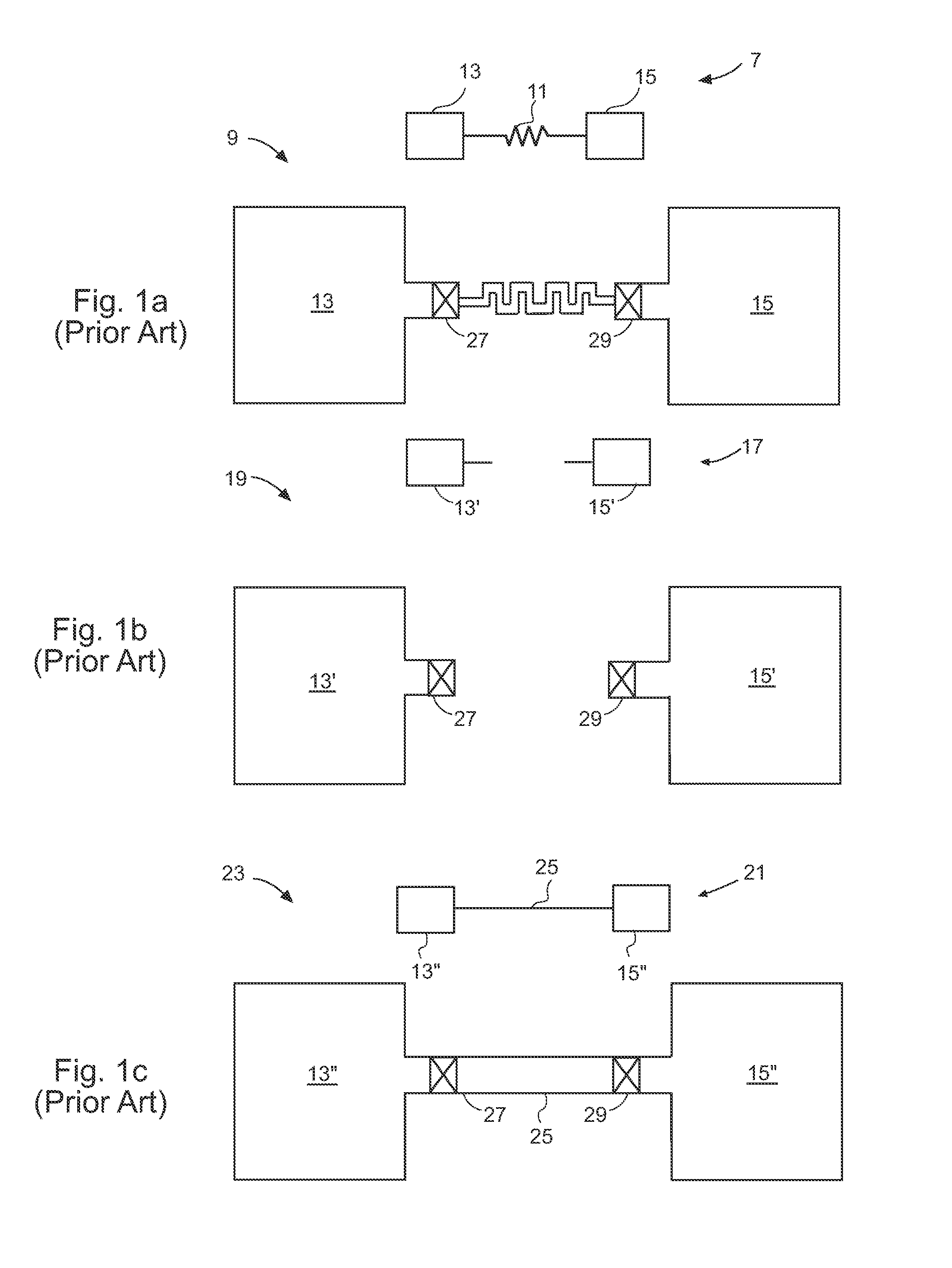
However the test pads, signal routing path, and test probes of the characterization test equipment (or device tester) introduce additional loading effects that can alter the DUT's performance.
Therefore, the results observed by the device tester may not accurately reflect the device's true performance.
Since there may be many different devices of different sizes in any one circuit design, this process can be very time consuming.
But this underscores the problem since a separate test DUT would be required for each desired resistor of a given resistance value (i.e of a given size).
As a result, the observed test results would likely be inaccurate.
With reference to FIG. 5a, another problem associated with testing a DUT is that at high frequencies, electromagnetic radiation 70 will emanate from a signal input or output pad 71.
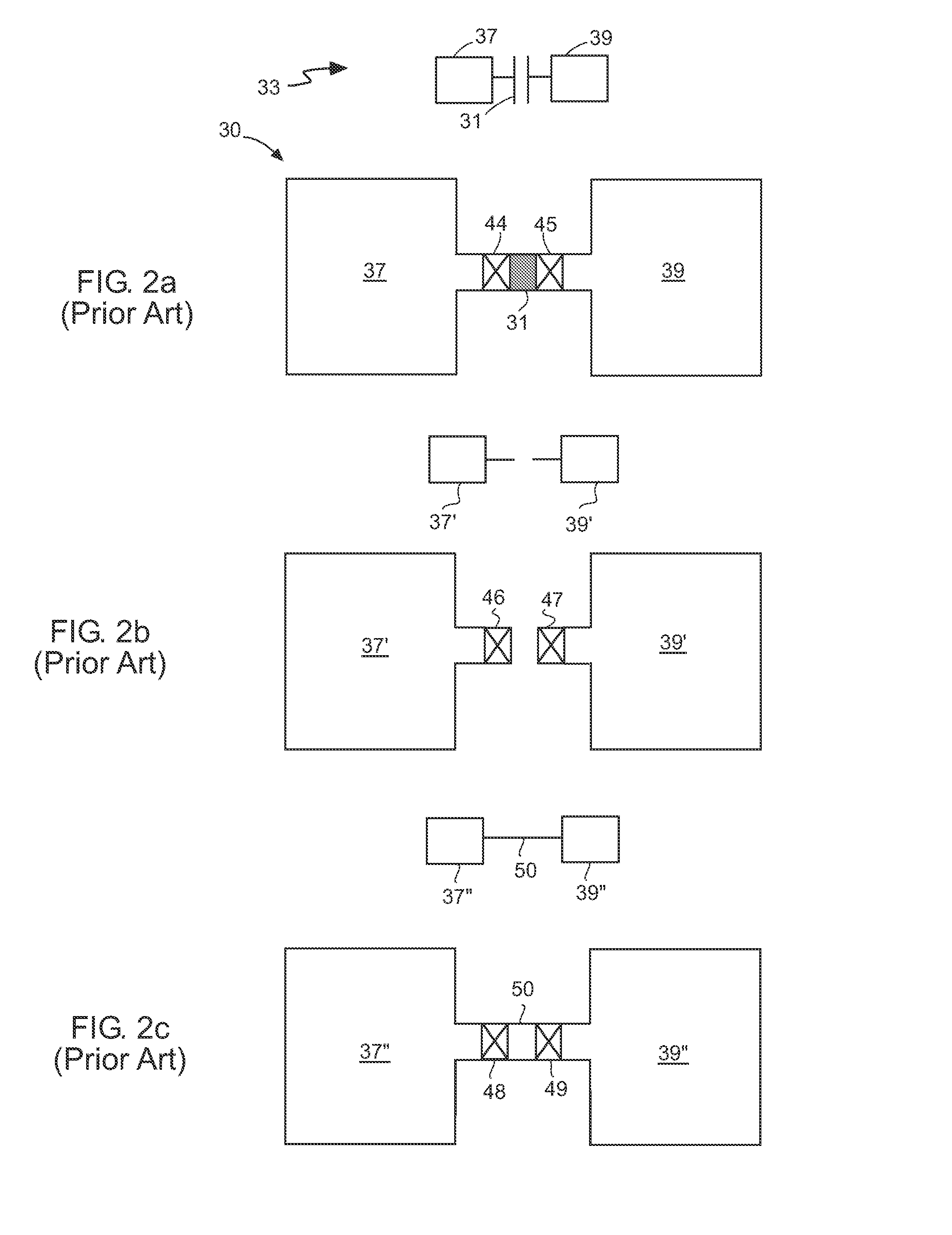
Consequently, the test pad configurations of FIGS. 1a–1c, 2a–2c, 3a–3c, and 4a–4c are actually not suitable for high frequency VNA applications.
This further complicates their construction and increases the size of test pad configuration.
As explained above, the problems of de-embedding test pad and test probe components from an electrical characterization procedure for a DUT is particularly acute in high frequency (commonly referred to as RF) chip designs, which require many different test structures in order to accurately model the various components that comprise the chip.
Due to this limitation, every DUT requires its own set of open-circuit and short-circuit test layout with associated pad set, consumes a lot of silicon area on a given test chip.

Method used


Image

  • Universal padset concept for high-frequency probing
  • Universal padset concept for high-frequency probing
  • Universal padset concept for high-frequency probing

Examples


Embodiment Construction

[0055]With reference to FIG. 10, the present embodiment establishes a universal pad set whose wiring pattern, i.e. routing pattern, to each GSG pad set is such that more than one size, or type, of DUT can be wired to existing GSG pad sets, but only one open-circuit and short-circuit test pad pattern and VNA calibration is required to de-embed the test-bed's parasitics from all the DUTs for which the test GSG pad set is suitable. For example, the test pad configuration of FIG. 10 is shown suitable for multiple sizes of capacitors, or simple resistors (although capacitors will be used in the present exemplary discussion). That is, two GSG pad sets are shown for accessing both end nodes of a capacitor, although no capacitor is shown in FIG. 10. Pads 101–103 constitute a first GSG pad set, and pads 104–106 constitute a second GSG pad set, and together, pads 101–106 constitute one universal pad set. Pads 101, 103, 104, and 106 are ground pads coupled together, and pads 102 and 105 are si...


PUM


Abstract

A universal, substrate Padset for de-embedding pad and signal line parasitics has an input pad group including a first input signal pad and a first ground pad; an output pad group including a first output signal pad and a second ground pad; a first input-signal-routing network for routing the first input signal pad to a first input node of a first predetermined test device; a first output-signal-routing network for routing the first output signal pad to a first output node of the first predetermined test device; a second input-signal-routing network for routing the first input signal pad to a second input node of a second predetermined test device; and a second output-signal-routing network for routing the first output signal pad to a second output node of the second predetermined test device. The layout configuration of the first test device is different from the layout configuration of the second test device.

Description

BACKGROUND OF THE INVENTION[0001]1. Field of the Invention[0002]The present invention relates to the use of test pad sets and vector network analyzers to de-embed test pad, routing path, and tester probe parasitics from characteristic measurements of a device under test, DUT.[0003]2. Description of the Related Art[0004]Generally, each new integrated circuit (IC) manufacturing process requires that components built with the new IC process be characterized (i.e. their performance tested). This requires that test components (or device under test, DUT, components), along with test pads for accessing the DUTs, be constructed for each new IC process. Characterization test equipment is then used to probe the DUTs by means of test probes applied to the DUTs' access pads. For example, to test the resistance of a resistor of a given material construction and shape, a known voltage may be applied across the resistor's test pads, and the resultant current through it observed. If the resistor's ...

Claims


Application Information

Patent Timeline
IPC IPC(8): G01R31/26
CPCG01R27/32G01R35/007G01R31/2884G01R31/2822
Inventor HARGROVE, MICHAELSTAREGO, MICHAEL
Owner SEIKO EPSON CORP
Learn More