Method and apparatus for circuit design and retiming

a circuit and timing behavior technology, applied in the field of circuit design, can solve the problems of difficult modelling of interconnection delays and thus often ignored

Active Publication Date: 2007-01-09
SYNOPSYS INC
View PDF4 Cites 20 Cited by
  • Summary
  • Abstract
  • Description
  • Claims
  • Application Information

AI Technical Summary

Benefits of technology

[0014]In one embodiment of the present invention, a method to design a circuit module includes: generating a plurality of circuit designs for a module, which corresponds to the module with a plurality of different latencies; determining a plurality of admissible clocks (e.g., minimum clock periods) for the plurality of circuit designs to represent the feasible clock periods for the plurality of circuit designs; and, generating design data to relate the plurality of admissible clocks with the plurality of different latencies. In one example, placement and routing are performed to generate each of the plurality of circuit designs; and, the admissible clocks are determined from detailed timing analyses based on the design layout. In one example, after a first one of the plurality of circuit designs is generated, a pipeline register set is inserted into the first one of the plurality of circuit designs to generate a second one of the plurality of circuit designs; and, retiming is further performed to generate the second one of the plurality of circuit designs. In one example, a first one of the plurality of circuit designs and a second one of the plurality of circuit designs have different architectures (e.g., having different processing logic or different logic processing elements). In one example, the design data further relates the plurality of different latencies with one or more data flow graph representations of the plurality of the circuit designs based on the plurality of admissible clocks. In one example, one or more data flow graph representations of the module are generated to represent the plurality of circuit designs based on the plurality of admissible clocks. For example, when a first one of the plurality of circuit designs includes a non-registered input, the one or more data flow graph representations include a representation of a computation node that represents at least a portion of signal delay on a first path in the first one of the plurality of circuit designs, where the first path contains no register and connects to the non-registered input; for example, the computation node represents the signal delay on the first path that is not smaller than signal delay on any path that contains no register and that connects between the non-registered input and a register in the first one of the plurality of circuit designs. Similarly, for example, when a first one of the plurality of circuit designs includes a non-registered output, the one or more data flow graph representations include a representation of a computation node that represents at least a portion of signal delay on a first path on the first one of the plurality of circuit designs, where the first path contains no register and connects to the non-registered output; and, for example, the computation node represents the signal delay on the first path that is not smaller than signal delay on any path that contains no register and that connects between the non-registered output and a register in the first one of the plurality of circuit designs. A computation node can also be used to represent the signal delay on the first path that is not smaller than signal delay on any path that contains no register and that connects the non-registered input and output in the first one of the plurality of circuit designs. In one example, a first graph representation of the one or more data flow graph representations corresponds to a first one of the plurality of circuit designs; the first graph representation includes an edge representing all first paths which start from and end in registers in the first one of the plurality of circuit designs; and, delay on the edge relates to a latency for the first one of the plurality of circuit designs. In one example, the edge connects a first node and a second node to represent the first paths, where the first node and the second nodes cause no signal delay.
[0015]In one embodiment of the present invention, a method to design a circuit includes: selecting a target clock for a design of the circuit; determining a representation of a data flow graph for a portion of the circuit based on the target clock; and retiming the design for the target clock using the representation of the data flow graph. In one example, a number of extra delays required on an edge of the data flow graph is determined based on the target clock in determining the representation of the data flow graph. In one example, the edge connects a first node and a second node of the data flow graph; the first and second nodes connected by the edge represent the paths that start from and end in registers in the portion of the circuit; the first node connects to a node that represents signal delay which is not smaller than signal delay on any path that contains no registers and that is between a first input of the portion of the circuit and an input of a register of the portion of the circuit; the second node connects to a node that represents signal delay which is not smaller than signal delay on any path that contains no registers and that is between a first output of the portion of the circuit and an output of a register of the portion of the circuit; and, the data flow graph comprises a node that represents signal delay which is not smaller than signal delay on any path that contains no registers and that connects one input of the portion of the circuit to one output of the portion of the circuit. In one example, retiming is performed on the portion of the circuit according to the target clock in determining the number of extra delays. In one example, the number of extra delays is determined from design data that correlates the numbers of extra delays with admissible clocks for the portion of the circuit.

Problems solved by technology

Interconnect delays are hard to model and thus often ignored.

Method used


Image

  • Method and apparatus for circuit design and retiming
  • Method and apparatus for circuit design and retiming
  • Method and apparatus for circuit design and retiming

Examples


Embodiment Construction

[0031]The following description and drawings are illustrative of the invention and are not to be construed as limiting the invention. Numerous specific details are described to provide a thorough understanding of the present invention. However, in certain instances, well known or conventional details are not described in order to avoid obscuring the description of the present invention. References to an or one embodiment in the present disclosure are not necessary to the same embodiment; and, such references means at least one.

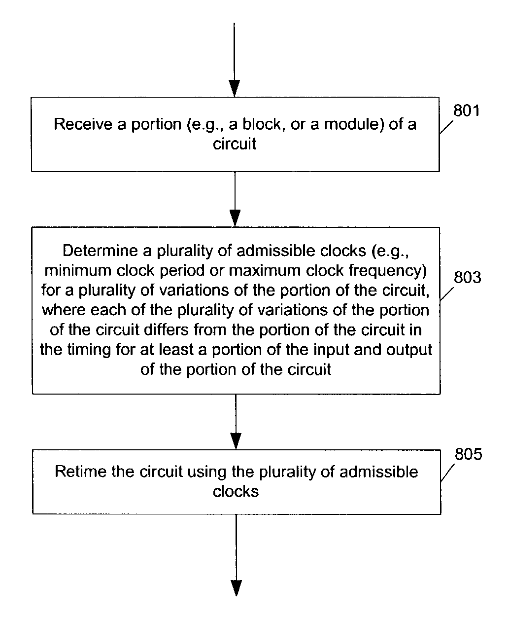
[0032]At least one embodiment of the present invention seeks to use a hierarchical method to retime a circuit design, in which a portion of the circuit (e.g., a circuit module or a circuit block) is retimed for clock period minimization and the entire circuit is retimed based on the result of the retiming of the portion of the circuit. In one embodiment of the present invention, a parametric design of a module is obtained to establish a timing model of the mod...


PUM


Abstract

Methods and apparatuses to hierarchically retime a circuit. In at least one embodiment of the present invention, a module of a circuit is designed with a plurality of different latencies to have a plurality of different minimum clock periods (e.g., through retiming at the module level). In one example, the minimum clock periods are determined from detailed timing analyses after the placement and routing for the module; and, in retiming the circuit that contains the module, a data flow graph representation of the module is constructed based on the target clock period of the circuit and the correlation between the latencies and the minimum clock periods. In at least one embodiment of the present invention, hierarchical retiming is performed in which portions of the circuit is retimed to generate results (e.g., for different latencies), which are selectively used for the retiming of the entire circuit based on the target clock period.

Description

FIELD OF THE INVENTION[0001]The invention relates to circuit design, and more particularly to the modeling of the timing behavior of circuit modules in circuit design.BACKGROUND[0002]For the design of digital circuits (e.g., on the scale of Very Large Scale Integration (VLSI) technology), designers often employ computer aided techniques. Standard languages such as Hardware Description Languages (HDLs) have been developed to describe digital circuits to aid in the design and simulation of complex digital circuits. Several hardware description languages, such as VHDL and Verilog, have evolved as industry standards. VHDL and Verilog are general purpose hardware description languages that allow definition of a hardware model at the gate level, the register transfer level (RTL) or the behavioral level using abstract data types. As device technology continues to advance, various product design tools have been developed to adapt HDLs for use with newer devices and design styles.[0003]In de...

Claims


Application Information

Patent Timeline
Patent Type & Authority Patents(United States)
IPC IPC(8): G06F17/50
CPCG06F17/5059G06F17/505G06F30/327G06F30/35
Inventor OKTEM, LEVENT
Owner SYNOPSYS INC
Why Eureka
Try Eureka