

Magnetic recording medium
a recording medium and magnetic technology, applied in the field of magnetic recording mediums, can solve the problems of inadequate noise reduction for applications, and achieve the effect of reducing the noise of the medium and high density recording
- Summary
- Abstract
- Description
- Claims
- Application Information
AI Technical Summary
Benefits of technology
Problems solved by technology
Method used
Image

Examples
example 1
[0027]A sputtering chamber was evacuated to a base pressure of 1×10⁻⁶ Torr, and then film forming was carried out as described below in an atmosphere of 5 mTorr at a substrate temperature of 220° C. by applying a substrate bias of −200V.
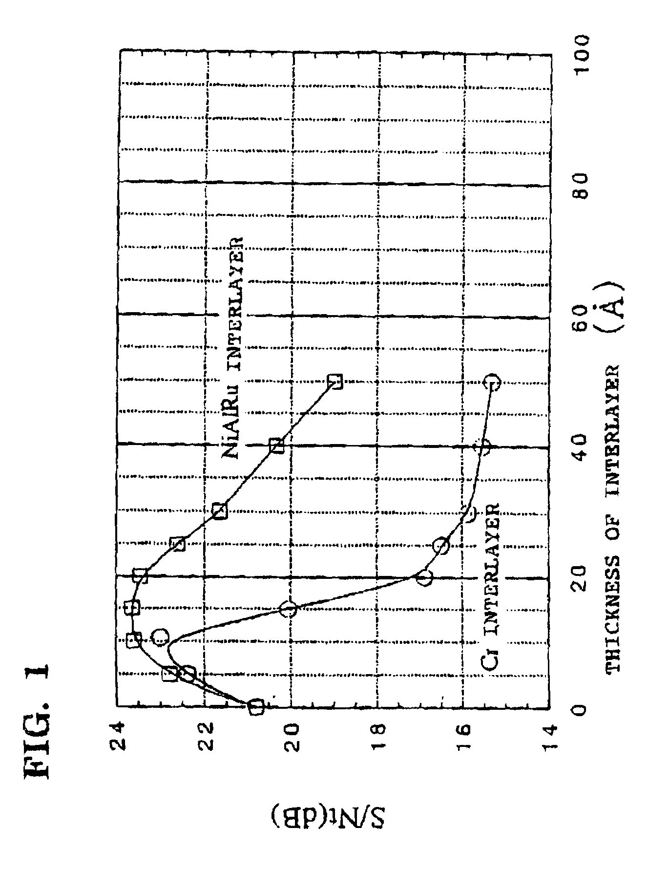
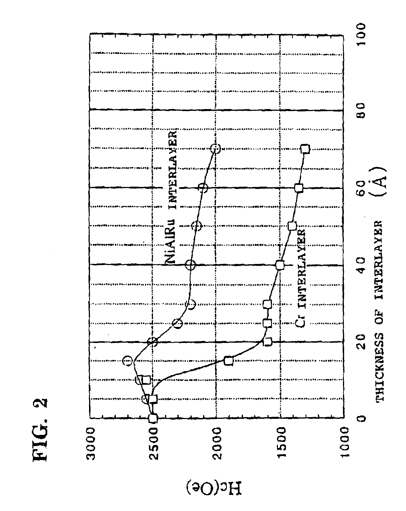
[0028]On a NiP / Al substrate having texture treatment applied thereto, a CrMo layer (thickness: 300 Å) was formed as an underlayer by a magnetron sputtering method using a target made of Cr85Mo15. Then, on the CrMo layer, a first magnetic layer made of Co71Cr17Ta5Pt7 (the amount of the respective components being atomic %) was formed in a thickness of 110 Å by a sputtering method. Then, a NiAlRu interlayer was formed thereon in a thickness within a range of from 5 Å to 70 Å by means of a Ni45Al50Ru5 target. Further, a second magnetic layer made of Co71Cr17Ta5Pt7 was formed thereon in a thickness of 110 Å by a similar operation. Then, a carbon type protective film and a lubricating film were formed thereon to obtain a test sample of Example 1 of the ma...
example 2
[0035]A sputtering chamber was evacuated to a base pressure of 1×10⁻⁶ Torr, and then film forming was carried out as described below in an Ar atmosphere of 5 mtorr at a substrate temperature of 270° C. without applying a substrate bias.
[0036]On a non-ferromagnetic substrate made of aluminosilicate glass, a NiAl seed layer (thickness: 500 Å) was firstly formed by a magnetron sputtering method using a target made of Ni50Al50 having B2 structure, and then a Cr layer (thickness: 300 Å) was formed as an underlayer.
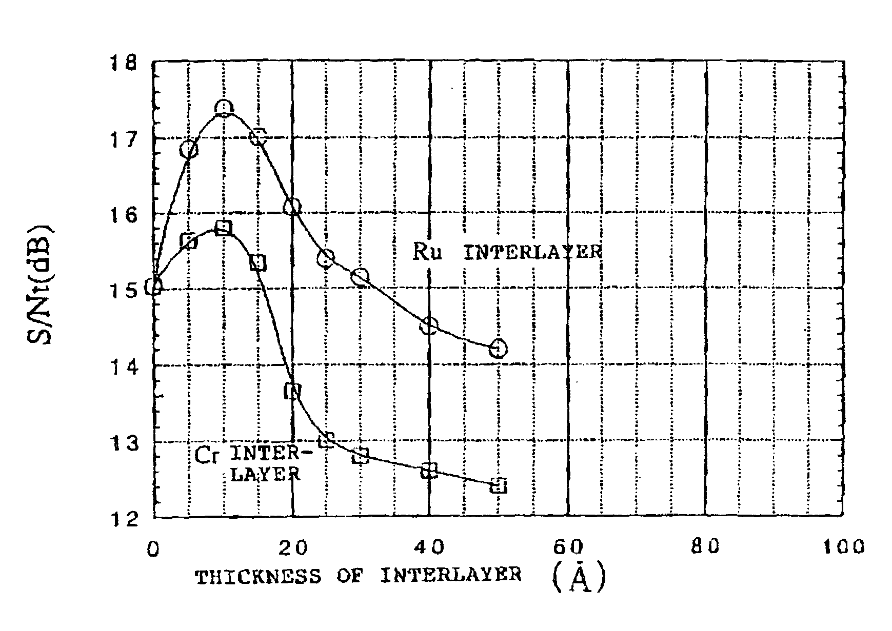
[0037]Then, on the Cr layer, a first magnetic layer made of Co71Cr17Ta4Pt8 (the amounts of the respective components being atomic %), was formed in a thickness of 110 Å by a sputtering method. Then, a Ru interlayer was formed thereon in a thickness within a range of 5 Å to 50 Å by means of a Ru target. Further, a second magnetic layer made of Co71Cr17Ta4Pt8 was formed thereon in a thickness of 110 Å by a similar operation. Then, a carbon type protective layer and a lubricating ...
example 3
[0044]A sputtering chamber was evacuated to a base pressure of 1×10⁻⁶ Torr, and then film forming was carried out as described below in an Ar atmosphere of 5 mTorr at a substrate temperature of 270° C. without applying a substrate bias.
[0045]On a non-ferromagnetic substrate made of aluminosilicate glass, a NiAl seed layer (thickness: 500 Å) was firstly formed by a magnetron sputtering method using a target made of Ni50Al50 having B2 structure, and then a Cr85Mo15 layer (thickness: 10 Å) was formed as an underlayer.
[0046]Then, on the CrMo layer, a first magnetic layer made of Co68Cr20Ta2Pt10 (the amounts of the respective components being atomic %), was formed in a thickness of 110 Å by a sputtering method. Then, a Ru interlayer was formed thereon in a thickness of 10 Å (i.e. the thickness of the Ru interlayer in which the maximum value of S / Nt was obtained in Example 2) by means of a Ru target. Further, a second magnetic layer made of Co68Cr20Ta2Pt10 was formed thereon in a thicknes...
PUM
| Property | Measurement | Unit |
|---|---|---|
| thickness | aaaaa | aaaaa |
| temperature | aaaaa | aaaaa |
| pressure | aaaaa | aaaaa |
Abstract
Description
Claims
Application Information