Charge pump bias network

a charge pump and bias network technology, applied in electronic switching, pulse automatic control, pulse technique, etc., can solve problems such as adversely affecting other sensitive components of the pll, and achieve the effect of minimizing current switching effects and eliminating noise effects

Active Publication Date: 2007-01-23
NORTHROP GRUMMAN SYST CORP
View PDF3 Cites 21 Cited by
  • Summary
  • Abstract
  • Description
  • Claims
  • Application Information

AI Technical Summary

Benefits of technology

[0004]The present invention resides in a charge pump bias network that can be coupled to any of a variety of differently configured charge pump circuits, to reduce or eliminate unwanted noise components that would otherwise be introduced by switching operations of the charge pump circuit. Briefly, and in general terms, the charge pump bias network of the present invention comprises a power supply; a first circuit for drawing a desired current from the power supply to a charge pump circuit, based on a digital control signal indicative of a currently desired current setting for the charge pump circuit; and a second circuit, interconnected with the first circuit, for drawing a complementary current from the power supply to a replica charge pump circuit. A practically constant total current is drawn from the power supply, regardless of fluctuations in the desired current setting for the charge pump circuit, as reflected in the digital control signal. Therefore, abrupt changes in power supply current are avoided and resultant switching noise effects are minimized. The terms “replica charge pump circuit” and “electrical replica of the charge pump circuit” as used in this description are intended to mean either a circuit that duplicates all the components of the charge pump circuit, or a circuit or load that has essentially the same electrical characteristics as the charge pump circuit. In many instances, the replica charge pump circuit may be simply a “dummy” electrical load with impedance characteristics that mimic those of the charge pump circuit.
[0008]The invention may also be defined as a method for minimizing current switching effects in a charge pump circuit. The method comprises the steps of representing a desired charge pump current setting as digital word; generating a set of current signals proportional to binary-weighted components corresponding to the digital word; applying the set of current signals to a set of two-position switches, each with first and second output terminals; applying the digital word as a set of binary signals to control the set of two-position switches and thereby switching each of the binary-weighted current signals to the first or second output terminal of each corresponding switch; combining output currents from the first output terminals of the switches and applying the result as a first common current signal to a first current mirror; and combining output currents from the second output terminals of the switches and applying the result as a second common current signal to a second current mirror. The method further comprises mirroring, in the first current mirror, the first common current signal to the charge pump circuit; and mirroring, in the second current mirror, the second common current signal to a replica of the charge pump circuit. The current mirrored to the replica of the charge pump circuit is complementary to the current mirrored to the charge pump circuit, in the sense that the two currents always sum to a constant current drawn from a common power supply.
[0009]It will be appreciated from the foregoing that the present invention represents a significant advance in charge pump circuits, as used in conjunction with phase-locked loops (PLLs). In particular, the charge pump bias network of the invention minimizes or eliminates noise effects resulting from current switching operations of a charge pump circuit. Other aspects and advantages of the invention will become apparent from the following more detailed description, taken in conjunction with the accompanying drawings.

Problems solved by technology

These switching operations necessarily result in abrupt changes in total current drawn by the charge pump circuit, and these abrupt current changes result in noise components that can modulate onto the power supply itself and adversely affect other sensitive components of the PLL.

Method used


Image

  • Charge pump bias network
  • Charge pump bias network
  • Charge pump bias network

Examples


Embodiment Construction

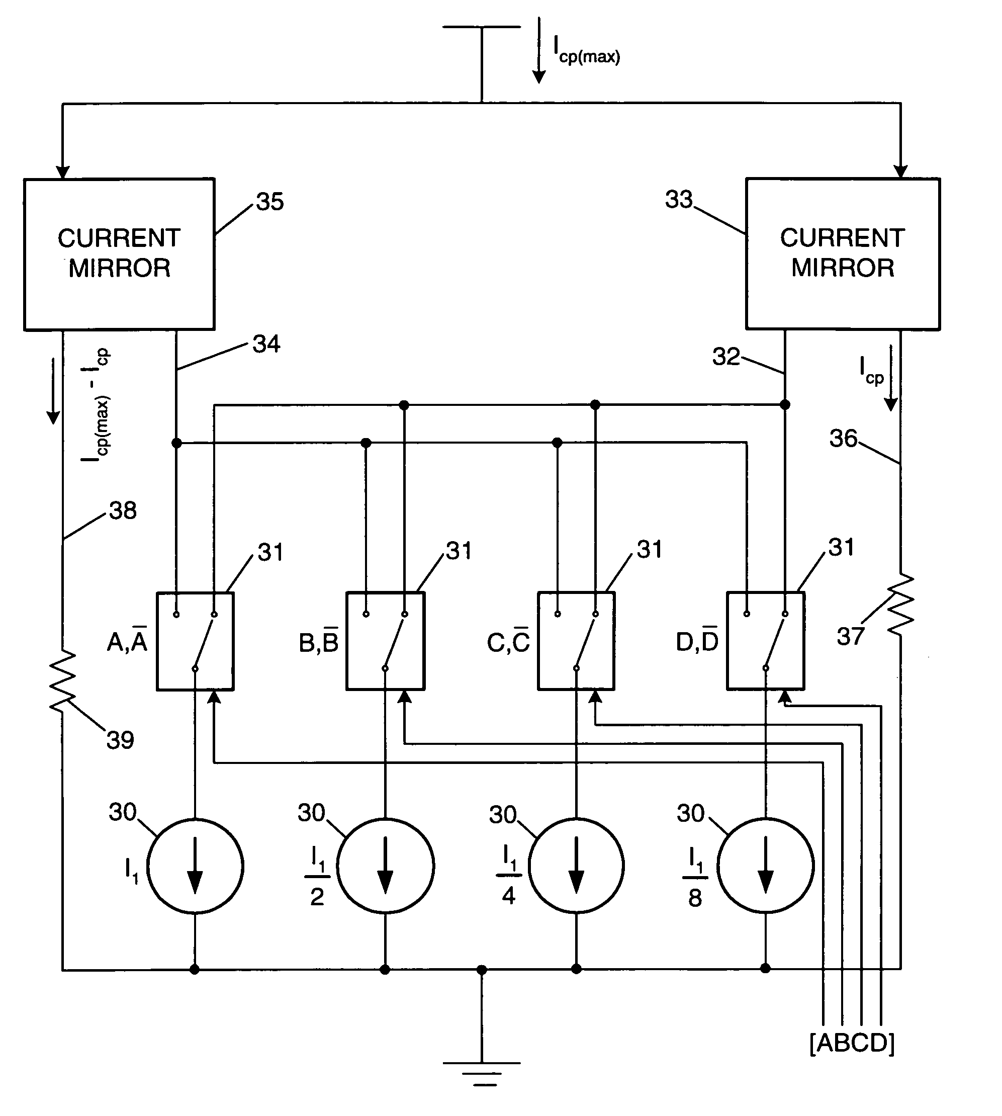
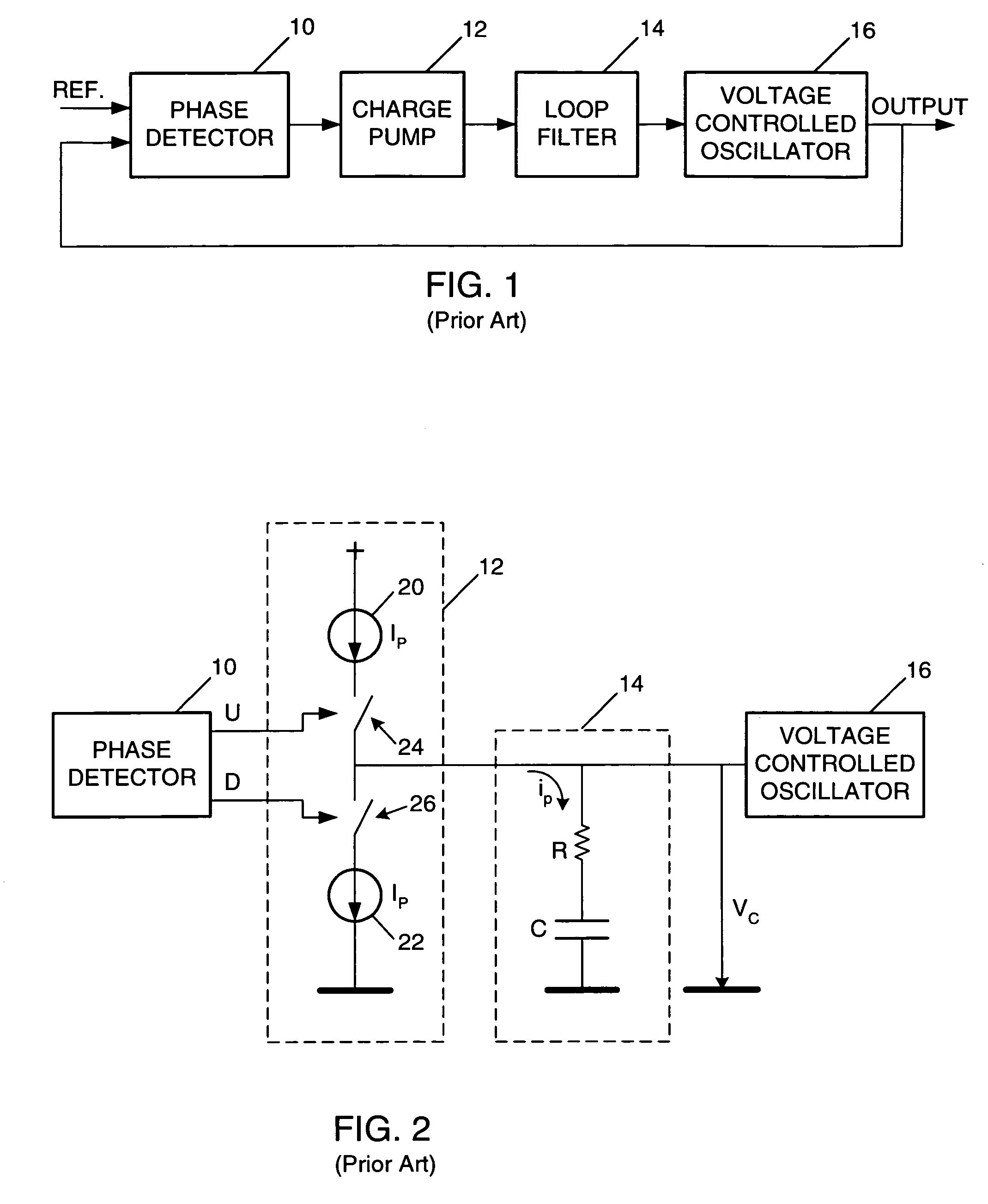
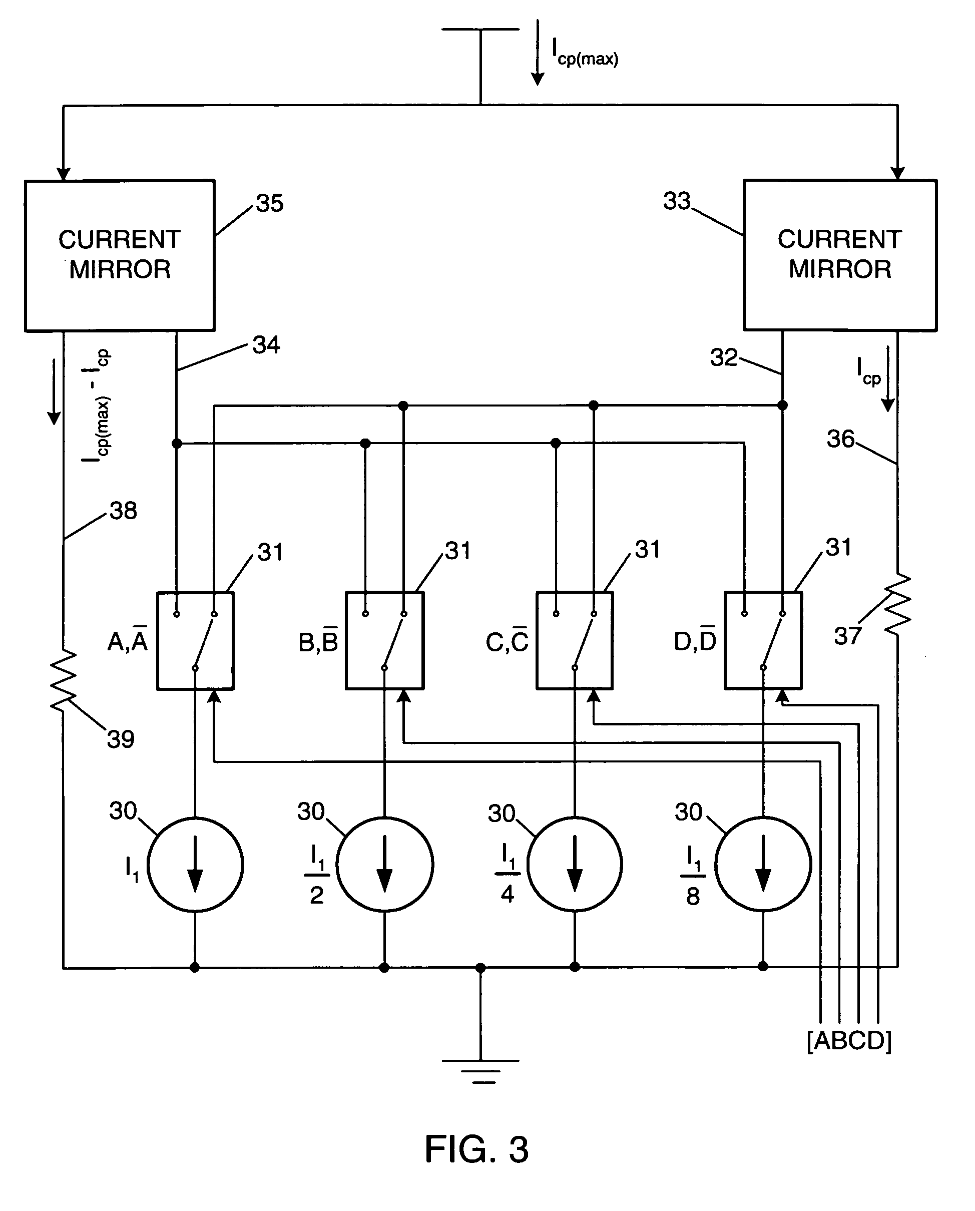
[0014]As shown in the drawings for purposes of illustration, the present invention is concerned with charge pump circuits as used in phase-locked loops (PLLs). FIG. 1 shows the basic components of a PLL, including a phase detector 10, a charge pump 12, a loop filter 14 and a voltage-controlled oscillator (VCO) 16. The VCO 16 generates an output signal at a desired frequency and also feeds back this signal to the phase detector 10. If, for example, the phase of the oscillator output signal falls behind the phase of a reference signal applied to the phase detector 10, the phase detector causes the charge pump to increase its output, which is used to control the VCO to speed up the output signal. Similarly, if the output signal from the VCO 16 leads the phase of the reference signal, the phase detector 10 causes the charge pump circuit 12 to slow the VCO 16. The loop filter 14 is basically a low-pass filter that smoothes out the abrupt control signals from the charge pump 12. This feed...


PUM


Abstract

A circuit for supplying selected currents to a charge pump without harmful effects arising from operation of current switches in the charge pump. A charge pump current setting is applied in digital form to a set of two-position switches coupled to binary-weighted current sources. Currents from the sources selected by the switches are combined, and the total current is mirrored to the charge pump. Simultaneously, those of the binary-weighted current sources not selected by the switches to contribute to the charge pump current are separately combined, and this total current is mirrored to an electrical replica of the charge pump. Thus the currents supplied to the charge pump and to the replica charge pump are complementary in the sense that they always add to a constant total current drawn from a common power supply. Therefore, abrupt changes in current load are avoided and switching noise effects are minimized.

Description

BACKGROUND OF THE INVENTION[0001]This invention relates generally to circuits known as charge pumps and, more particularly, to charge pumps as used in conjunction with phase-locked loops (PLLs). Phase-locked loops are widely used in a variety of applications in which a time-varying signal must be synchronized (locked) with a reference signal. Typical applications include frequency synthesizers for radio receivers and transmitters, demodulation of radio signals, and recovery of clock timing information from received radio signals or from digital storage devices. A common PLL configuration includes a phase detector, a charge pump, a loop filter, and a voltage controlled oscillator, the output of which is fed back as an input to the phase detector. The theory of operation of PLL circuits that include a charge pump is well known in the art. Basically, the phase detector generates signals indicative of the phase difference between a time-varying signal and a reference signal. Then the ch...

Claims


Application Information

Patent Timeline
Patent Type & Authority Patents(United States)
IPC IPC(8): H03K17/16H03L7/093
CPCH03L7/0898
Inventor RODGERS, PAUL L.GOYETTE, WILLIAM R.
Owner NORTHROP GRUMMAN SYST CORP
Why Eureka
Try Eureka