Method for making an integrated active antenna element

a technology of active antenna elements and integrated circuits, which is applied in the direction of resonance antennas, waveguide type devices, substation equipment, etc., can solve the problems of being expensive by comparison with reflector antenna types, the cost of microwave monolithic integrated circuits (mmics) was a major cost obstacle, and the cost of tr modules and antenna structures were secondary

Inactive Publication Date: 2007-01-30
LOCKHEED MARTIN CORP
View PDF8 Cites 29 Cited by
  • Summary
  • Abstract
  • Description
  • Claims
  • Application Information

AI Technical Summary

Problems solved by technology

They have the disadvantage, in general, of being expensive by comparison with antenna types such as reflector antennas.
At one time, the cost of the microwave monolithic integrated circuit (MMIC) was a major cost obstacle, and other costs, such as the TR module and antenna structure, were secondary.

Method used


Image

  • Method for making an integrated active antenna element
  • Method for making an integrated active antenna element
  • Method for making an integrated active antenna element

Examples


Embodiment Construction

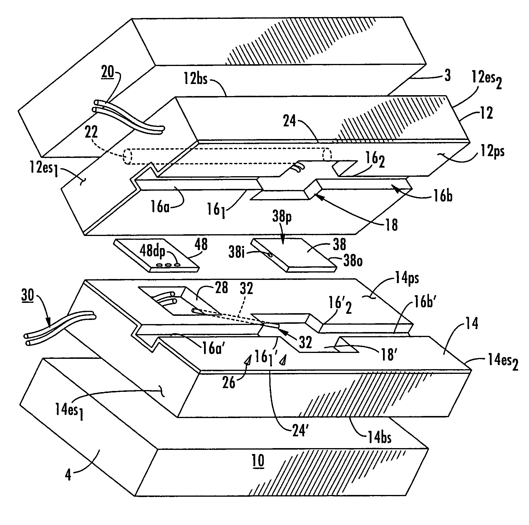
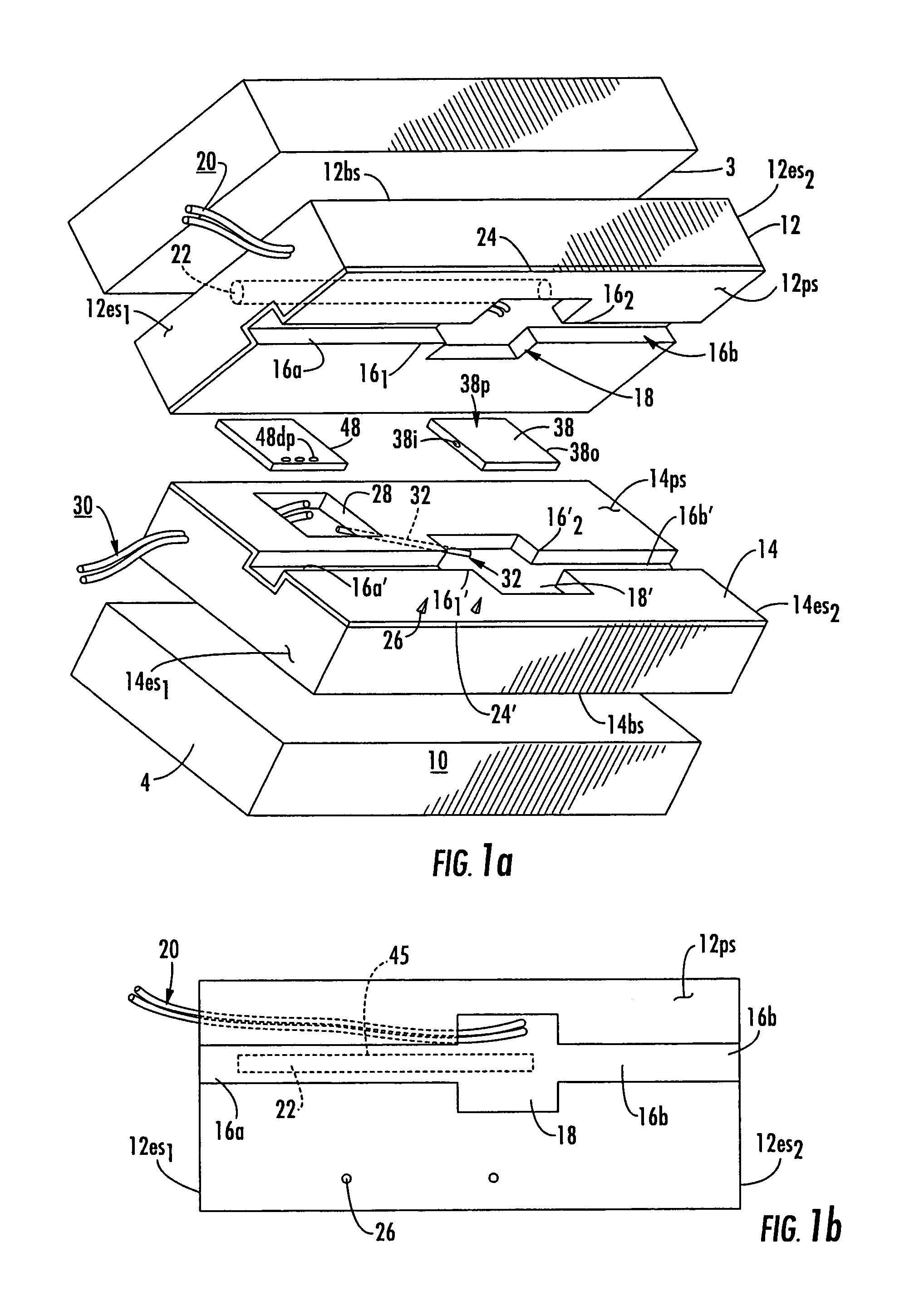
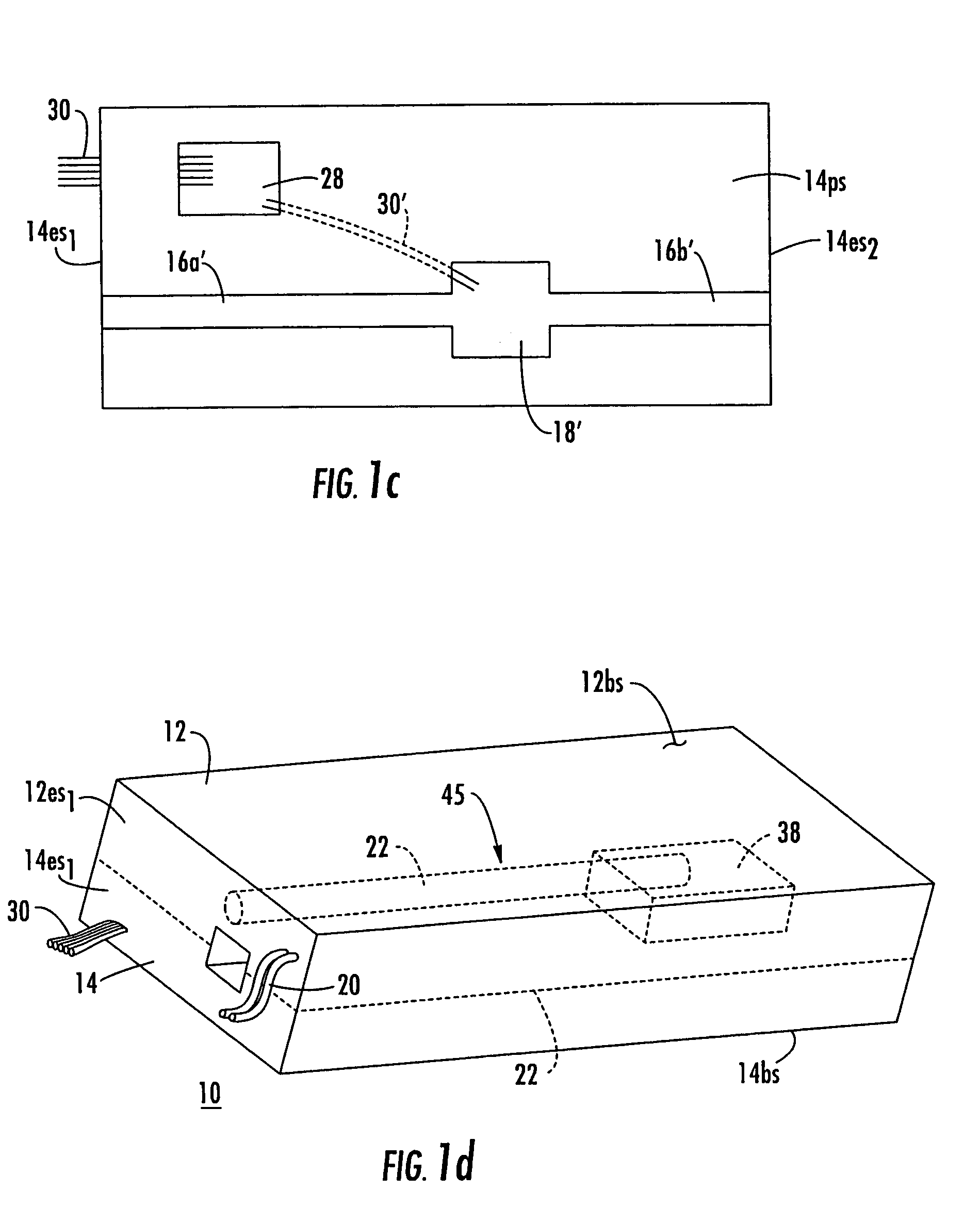
[0018]In FIGS. 1a, 1b, 1c, and 1d, a structure 10 includes an upper dielectric slab 12 and a lower dielectric slab 14. In this context, the terms “upper” and “lower” refer to the position of the elements in the drawings, and are not intended to indicate the position of the actual element when fabricated or in use. The dielectric materials of the upper and lower slabs may be the same or they may be different, and the slab itself may be made by machining from a larger mass of dielectric material, or it may made by hardening a liquid molding material in a mold. The molds in which the upper and lower slabs 12 and 14, respectively, may be formed are illustrated as 3 and 4, respectively.

[0019]Dielectric slab 12 defines a planar surface 12ps and a back surface 12bs, and end surfaces 12es1 and 12es2. A depression or recess 18 is defined in planar surface 12ps. As illustrated, the recess 18 is generally rectangular, and is not so deep as to open to rear or back surface 12bs. A first channel ...


PUM

PropertyMeasurementUnit
power electrical conductoraaaaaaaaaa
electrically conductiveaaaaaaaaaa
relative phase shiftsaaaaaaaaaa

Abstract

An array of electrically conductive waveguides is made by a method including defining slots in broad surfaces of planar dielectric slabs. The surfaces of the slabs, including slots, are metallized. The broad sides of the slabs are juxtaposed, with the slots registered with the planar surfaces of another slab, to form one or more closed waveguides. Heat pipes are made by defining apertures within the dielectric slabs, and introducing wick material into the apertures.

Description

FIELD OF THE INVENTION[0001]This invention relates to active array antennas, and more particularly to active transmit, receive, or transmit-receive modules or elements which are encapsulated in dielectric material.BACKGROUND OF THE INVENTION[0002]Active antenna arrays are increasingly required for sensors, communications, and electronic warfare systems. Active antenna arrays are arrays of antenna elements in which each antenna element or subset of antenna elements is driven by, or drives, one or more active radio-frequency (RF) device(s) such as a monolithic microwave integrated circuit (MMIC). Some prior art arrangements associate a transmit-receive (TR) module with each antenna element, as described in U.S. Pat. No. 5,017,927, issued May 21, 1991 in the name of Agrawal et al. or with a subset of antenna elements of the array, as described in U.S. Pat. No. 5,339,086, issued Aug. 16, 1994 in the name of DeLuca et al. Active array antennas are advantageous in that their beams can be ...

Claims


Application Information

Patent Timeline
Patent Type & Authority Patents(United States)
IPC IPC(8): H01P11/00
CPCH01Q13/0283H01Q23/00Y10T29/49085Y10T29/49002Y10T29/49083Y10T29/49016Y10T29/49018Y10T29/49082
Inventor EHRET, TIMOTHYSMITH, BRADLEY M.
Owner LOCKHEED MARTIN CORP
Why Eureka
Try Eureka