Chip select method through double bonding

a technology of double bonding and select method, which is applied in the direction of logic circuit, semiconductor/solid-state device details, pulse technique, etc., can solve the problems of increasing the cost of the device, and achieve the effect of simplifying qualification, simplifying testing, and reducing overall costs

Active Publication Date: 2007-01-30
MONTEREY RES LLC
View PDF10 Cites 14 Cited by
  • Summary
  • Abstract
  • Description
  • Claims
  • Application Information

AI Technical Summary

Benefits of technology

[0005]The objects, features and advantages of the present invention include providing a method and / or architecture for a configurable chip that may (i) be configured as one of several different devices, (ii) minimize overall costs, (iii) simplify qualification, (iv) simplify testing and / or (v) allow a single mask set to be used for multiple products.

Problems solved by technology

Treating each device of the family differently increases the costs of the devices.

Method used


Image

  • Chip select method through double bonding
  • Chip select method through double bonding
  • Chip select method through double bonding

Examples


Embodiment Construction

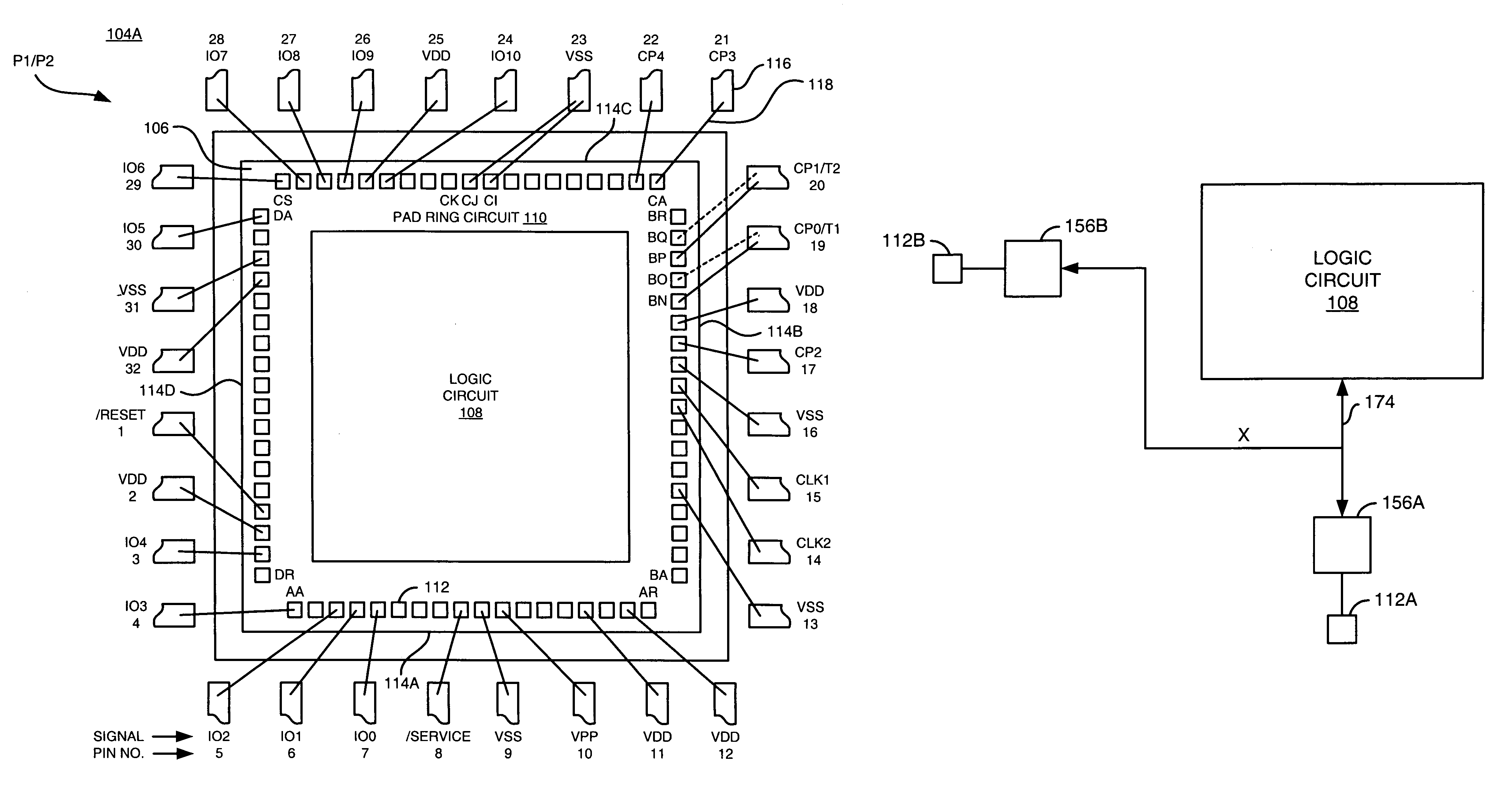
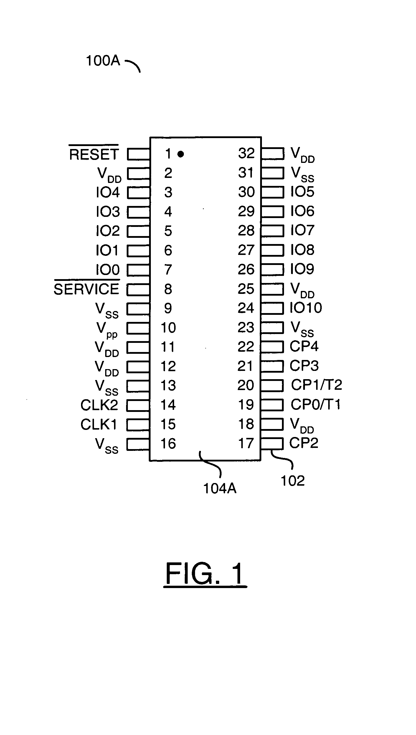
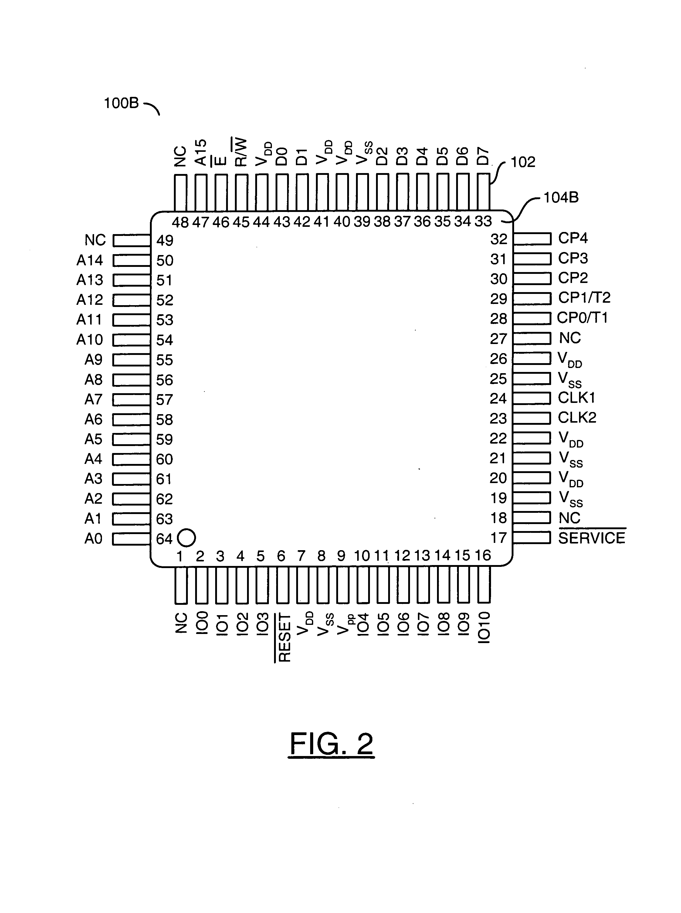
[0016]Referring to FIGS. 1 and 2, package drawings of a device 100A and a related device 100B are shown in accordance with a preferred embodiment of the present invention. Each of the devices 100A and 100B generally includes multiple pins, balls, tabs, solder bumps or similar elements for externally interfacing to the devices 100A and 100B. Hereafter, the various pins, balls, tabs, solder bumps and the like may be referred to generally as a pin 102, pins 102 and / or a specific pin X (where X is a pin number 1100A and 100B may also include a package 104. The device 100A may be implemented as a 32-pin small outline integrated circuit (SOIC) package 104A. The device 100B may be implemented as a 64-pin thin quad flat package (TQFP) 104B. Hereafter, the various package types 104A and 104B may be referred to generally as a package 104 and / or packages 104. Other packages 104 and / or pin configurations may be implemented to meet the design criteria of a particular application using the invent...


PUM


Abstract

A chip generally comprising a logic circuit and a plurality of pads. The logic circuit may be configured to operate in a plurality of modes in response to a mode signal. The pads may be configurable into a plurality of subsets such that one of the subsets is used by the logic circuit at a time in response to the mode signal.

Description

FIELD OF THE INVENTION[0001]The present invention relates to a method and / or architecture for configurable chips generally and, more particularly, to a method and / or architecture for configurable chips having different pad configurations in different modes.BACKGROUND OF THE INVENTION[0002]Manufacturers of semiconductor devices commonly produce a family of devices based on a core set of functionality. The different members of the family vary by packaging, pin assignments and numbers of special purpose input and / or output pins that tailor the devices to specific applications. Production of the various family members commonly involves production of a unique chip for each distinct device. The unique chips often vary from each other by one or more masks used in the fabrication processes.[0003]Since each chip family has a unique fabrication, the devices incorporating the chips remain unique throughout the life cycles of the devices. Therefore, each device type in the family commonly has a...

Claims


Application Information

Patent Timeline
Patent Type & Authority Patents(United States)
IPC IPC(8): H01L23/48H01L25/00
CPCH01L23/50H01L24/49H01L24/06H01L2224/05554H01L2224/0401H01L2224/48247H01L2224/49113H01L2224/49171H01L2924/01004H01L2924/01005H01L2924/01013H01L2924/01018H01L2924/0102H01L2924/01027H01L2924/01047H01L2924/01056H01L2924/01058H01L2924/01074H01L2924/01083H01L2924/014H01L2924/14H01L2924/19041H01L2924/19042H01L2924/19043H01L2924/3011H01L24/48H01L2924/01023H01L2924/01024H01L2924/01033H01L2924/01041H01L2924/01055H01L2924/00H01L2924/00014H01L2224/45099H01L2224/05599
Inventor SHAH, SHAILESH
Owner MONTEREY RES LLC
Why Eureka
Try Eureka