Dielectric waveguide filter

a filter and waveguide technology, applied in the direction of waveguides, electrical devices, coupling devices, etc., can solve the problems of low yield, high degree of variability in performance, and inability to meet the requirements of the filter, so as to reduce the number of filter stages, improve the effect of out-of-band suppression characteristics and compact devices

Inactive Publication Date: 2007-01-30
NEC CORP
View PDF8 Cites 29 Cited by
  • Summary
  • Abstract
  • Description
  • Claims
  • Application Information

AI Technical Summary

Benefits of technology

[0004]It is an object of the present invention to provide a dielectric waveguide filter that is capable of forming out-of-band attenuation poles without additionally forming openings for interlaced electromagnetic field coupling.
[0006]By two-dimensionally arranging resonators that are surrounded by via-holes, out-of-band attenuation poles can be formed without additionally providing openings for interlaced electromagnetic field coupling. As a result, the out-of-band suppression characteristic can be improved, the number of filter stages can be reduced, and a more compact device can be realized.
[0007]The formation of waveguide-coplanar converters on the dielectric resonators of the input and output stages of the filter enables flip-chip packaging. In addition, there is no need for providing openings on resonators other than the input and output stages, and this configuration is therefore less prone to misregistration between the conductive layers and via-holes during fabrication.

Problems solved by technology

As a result, misregistration between the via-holes and the conductive pattern tends to occur due to the degree of control of the coefficient of contraction during sintering.
As a consequence, problems are encountered in fabrication such as a high degree of variability in performance and low yield.

Method used


Image

  • Dielectric waveguide filter
  • Dielectric waveguide filter
  • Dielectric waveguide filter

Examples


first embodiment

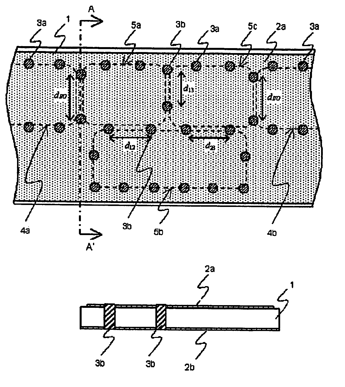
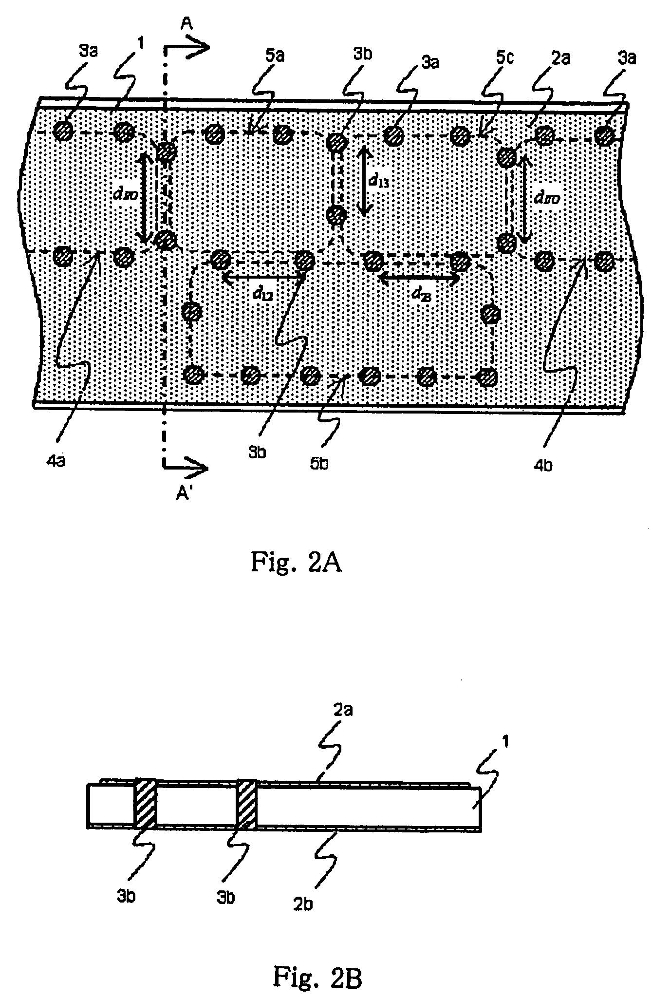
[0024]A first embodiment according to the present invention will now be explained in detail with reference to FIG. 2. FIG. 2A is a plan view of a filter substrate, and FIG. 2B is a sectional view taken along alternate long and short dash line A–A′ in FIG. 2A.

[0025]Upper and lower conductive layers 2a and 2b are formed on the upper and lower surfaces of dielectric substrate 1. Upper and lower conductive layers 2a and 2b are connected each other by via-hole rows 3a and 3b that are formed with a spacing being equal to or less than ½ of the wavelength in the dielectric substrate at the resonance frequency, whereby first-stage, second-stage, and third-stage dielectric resonators 5a, 5b, and 5c and input / output waveguide structures 4a and 4b are formed. The filter is configured such that first-stage resonator 5a and second-stage resonator 5b are coupled by an electromagnetic field by means of dielectric windows in the form of via-holes 3b with a spacing being equal to d12 and second-stage...

second embodiment

[0026]As the present invention, a configuration that allows regulation of the filter characteristics will be explained with reference to FIG. 3. FIG. 3A is a plan view of the filter substrate, FIG. 3B is a detailed view of the area 6 enclosed by the dotted lines in FIG. 3A, and FIG. 3C is a sectional view taken along alternate long and short dash line B–B′ in FIG. 3B.

[0027]Forming slot 7 around the periphery of via-hole 3a that forms a resonator causes pad 8 to be formed that is electrically isolated from conductive layer 2a. This pad 8 and conductive layer 2a are connected with each other by, for example, bonding wires 9. The number of wires or their length are regulated to form inductance regulator 6 for regulating the inductance of via-holes 3a that form the side walls of the dielectric resonator. Changes in the inductance change the resonance frequency of the dielectric resonator. Accordingly, forming inductance regulator 6 in each resonator stage enables regulation of the cente...

third embodiment

[0028]the present invention will now be explained in detail with reference to FIG. 4. FIG. 4A is a plan view of the filter substrate, and FIG. 4B is a sectional view taken along alternate long and short dash line C–C′ in FIG. 4A.

[0029]Upper and lower conductive layer 2a and 2b are formed on the surfaces of dielectric substrate 1. First-stage, second-stage, and third-stage dielectric resonators 5a, 5b, and 5c are formed by connecting these upper and lower conductive layers 2a and 2b by means of via-hole rows 3a and 3b that are formed with a spacing being equal to or less than ½ of the wavelength in the dielectric substrate at the resonance frequency. Formed on first-stage resonator 5a and third-stage resonator 5c are waveguide-coplanar converters 10 that are connected to input / output coplanar lines that are made up of ground conductive layer 2a and signal conductive layer 2c. The degree of electromagnetic field coupling between input / output stage resonators 5a and 5c and waveguide-co...


PUM


Abstract

A conductive layer is formed on each of the upper and lower surfaces of a dielectric substrate, and the two conductive layers are connected by rows of via-holes that are formed which a spacing that is less than or equal to ½ of the wavelength in the dielectric substrate in the resonance frequency, whereby n stages of dielectric resonators and input / output waveguide structures are formed. If the number n of stages is assumed to be 3, the first-stage resonator and the second-stage resonator are coupled by an electromagnetic field by means of via-holes of a first spacing; the second-stage resonator and the third-stage resonator are coupled by an electromagnetic by means of via-holes of a second spacing, whereby a filter is formed. The input / output waveguide structure and the filter are coupled by an electromagnetic by means of via-holes of a fourth spacing. The first-stage resonator and the third-stage resonator are coupled by an electromagnetic field by means of via-holes of a third spacing.

Description

TECHNICAL FIELD[0001]The present invention relates to a dielectric waveguide filter that has an upper conductive layer and a lower conductive layer on the surfaces of a dielectric substrate, wherein a row of via-holes or conductors that connect the upper conductive layer and lower conductive layer is used to form resonators and dielectric windows.BACKGROUND ART[0002]There exists a need for filters that feature low loss and a steep out-of-band suppression characteristic, and further, that feature compact size and connectability with a planar circuit. From the standpoint of connection reproducibility and low parasitic inductance at high frequencies, it is also strongly desired that such filters allow flip-chip packaging. One filter having these characteristics is shown in FIG. 1 and described in the public literature in a paper by M. Ito et al. (IEEE International Microwave Symposium Digest, pp. 1597–1600, May 2001). FIG. 1A is a plan view of this known example of a filter, and FIG. 1...

Claims


Application Information

Patent Timeline
Patent Type & Authority Patents(United States)
IPC IPC(8): H01P1/208H01P3/16H01P5/107
CPCH01P5/107H01P1/2088
Inventor ITO, MASAHARUMARUHASHI, KENICHIOHATA, KEIICHI
Owner NEC CORP
Why Eureka
Try Eureka