Sensor for inspection instrument and inspection instrument

a technology of inspection instruments and sensors, applied in the direction of instruments, individual semiconductor device testing, semiconductor/solid-state device testing/measurement, etc., can solve the problems of difficult assuring, inability to inspect circuit patterns in the level of 50 m with a high degree of resolution

Inactive Publication Date: 2007-02-06
OHT
View PDF14 Cites 54 Cited by
  • Summary
  • Abstract
  • Description
  • Claims
  • Application Information

AI Technical Summary

Benefits of technology

[0007]In order to solve the above problems of the conventional techniques, it is therefore an object of the present invention to provide...

Problems solved by technology

The recent progressive densification of conductive patterns causes difficulties in assuring a sufficient space for simultaneously arranging a plurality of pins, respectively, at the ends of adjacent conductive patterns and bringing the pins into contac...

Method used


Image

  • Sensor for inspection instrument and inspection instrument
  • Sensor for inspection instrument and inspection instrument
  • Sensor for inspection instrument and inspection instrument

Examples


Embodiment Construction

[0023]With reference to the drawings, an embodiment of the present invention will now be described in detail. While the following description is made in connection with a specific embodiment, the present invention is not limited to any structures, arrangements of components and numerical values of the specific embodiments, unless otherwise specified.

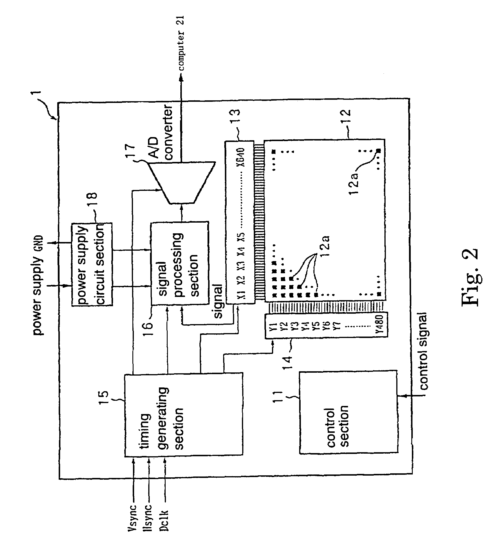
[0024]As one embodiment of the present invention, an inspection apparatus using a MOSFET as a sensor element will be described below.

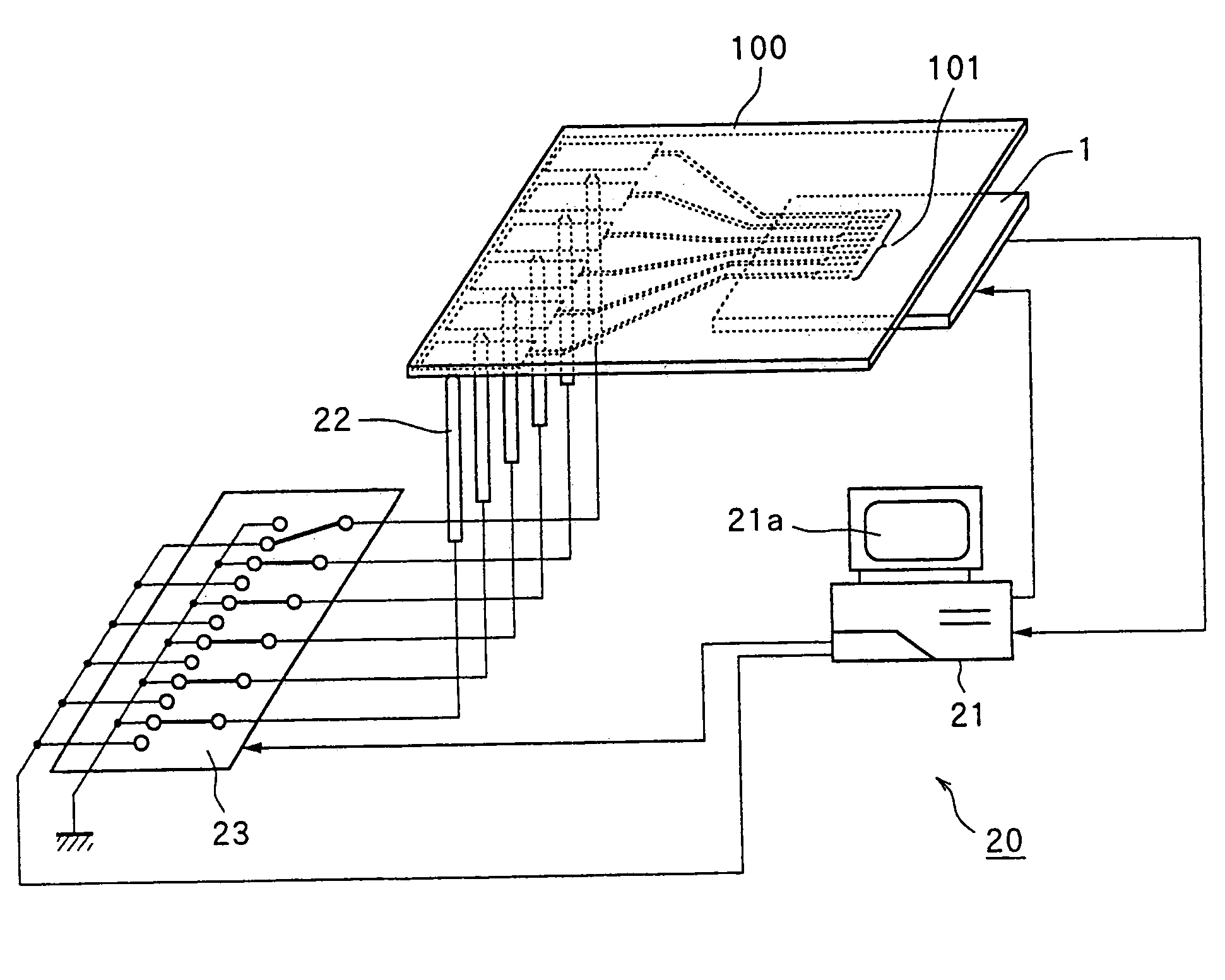
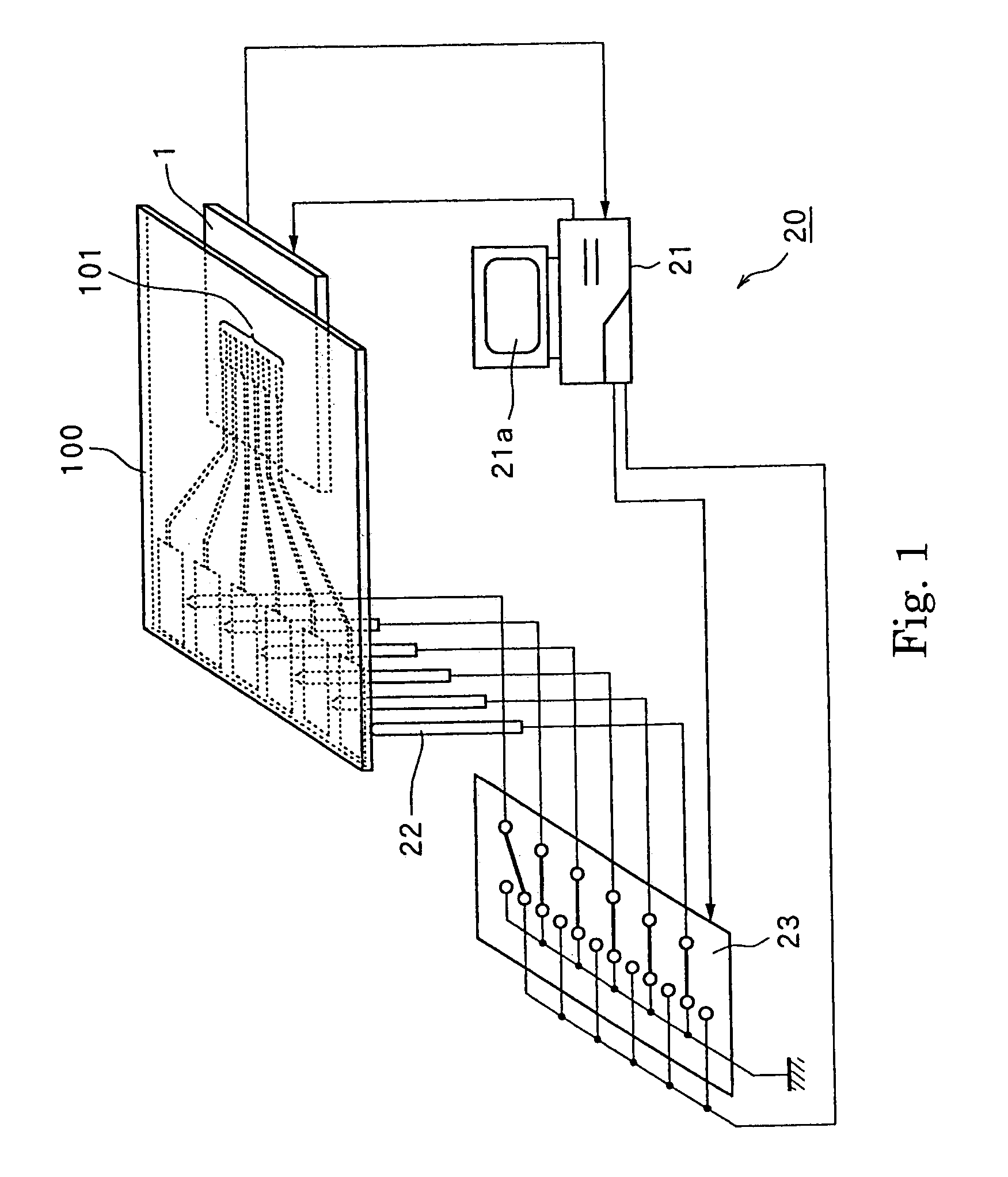
[0025]Referring to FIG. 1, an inspection system incorporating the inspection apparatus according to one embodiment of the present invention will first be schematically described.

[0026]In FIG. 1, the inspection system generally designated by the reference numeral 20 is designed to inspect a plurality of conductive patterns 101 formed on a circuit board 100. The inspection system 20 comprises an inspection apparatus 1, a computer 21, a plurality of probes 22 for supplying an inspection signal to the conductiv...


PUM


Abstract

Disclosed is an inspection sensor and inspection apparatus capable of accurately inspecting the shape of a conductive pattern. A sensor element 12a includes an MOSFET, and an aluminum electrode (AL) serving as a passive element 80. The passive element or aluminum electrode 80 is connected to the gate of a MOSFET 81 and the source of a MOSFET 82. A voltage VDD is supplied from a power supply circuit 18 to the drain of the MOSFET 81, and the source of the MOSFET 81 is connected to the drain of a MOSFET 83. A reset signal is entered from a vertical selection section 14 into the gate of the MOSFET 82, and the voltage VDD is supplied from the power supply circuit 18 to the drain of the MOSFET 82. A selection signal is entered from the vertical selection section 14 into the gate of the MOSFET 83, and an output from the source of the MOSFET 83 is entered into a lateral selection section 13.

Description

TECHNICAL FIELD[0001]The present invention relates to an inspection apparatus for a conductive pattern of a circuit board and to a sensor for the inspection apparatus.BACKGROUND ART[0002]In manufacturing processes of a circuit board, it is required to inspect the presence of disconnection and / or short-circuit in conductive patterns formed on a circuit board.[0003]As to a technique for inspecting a conductive pattern, there has been known a contact type inspection technique comprising bringing two pins into contact, respectively, with both ends of a conductive patter, supplying an electrical signal from one of the pins, and receiving the electrical signal by the other pin to inspect the presence of disconnection or the like in the conductive pattern.[0004]The recent progressive densification of conductive patterns causes difficulties in assuring a sufficient space for simultaneously arranging a plurality of pins, respectively, at the ends of adjacent conductive patterns and bringing ...

Claims


Application Information

Patent Timeline
IPC IPC(8): G01R31/00G01R31/28G01R31/02G01R31/312H01L21/822H01L27/04H05K3/00
CPCG01R31/312
Inventor FUJII, TATSUHISAMONDEN, KAZUHIROKASAI, MIKIYAISHIOKA, SHOGOYAMAOKA, SHUJI
Owner OHT
Why Eureka
Try Eureka