Dual layer signal processing in a layered modulation digital signal system

a digital signal and layered modulation technology, applied in the field of digital signal receiving systems, can solve the problems of limited electromagnetic spectrum availability, difficult to implement new services, and difficult to simply transmit enhanced or additional data at a new frequency, so as to achieve high-speed digital processing and minimize signal noise and cost.

Inactive Publication Date: 2007-02-06
HUGHES ELECTRONICS
View PDF159 Cites 58 Cited by
  • Summary
  • Abstract
  • Description
  • Claims
  • Application Information

AI Technical Summary

Benefits of technology

[0014]The present invention provides a flexible and expandable apparatus that can be implemented with high speed logic circuit capable of performing demodulator functions and processing of received layered modulation signals in real-time. The invention utilizes high speed digitization of the incoming signal to prepare it for further high speed digital processing. The digital processing demodulates and decodes the distinct layers of layered signal. The invention enables a receive system architecture wherein the incoming layered signal is processed by a single decoder to produce distinct layer signals for further decoding, thereby minimizing signal noise and cost. The processor can be included in a single integrated receiver / decoder (IRD) further comprising a separate transport for each decoded signal layer.

Problems solved by technology

However, it is more difficult to implement improvements in old systems and new services when it is necessary to replace existing legacy hardware, such as transmitters and receivers.
In the realm of wireless communications, this principle is further highlighted by the limited availability of electromagnetic spectrum.
Thus, it is not possible (or at least not practical) to merely transmit enhanced or additional data at a new frequency.
Unfortunately, QPSK receivers cannot demodulate 8PSK or 16QAM signals.
In addition, such receiver systems are limited because they are designed to only receive coherent layered signals, i.e. signals that are synchronously produced.
Furthermore, because additional signal processing usually introduces unwanted noise, it is also important to minimize the amount of processing performed on a received signal.

Method used


Image

  • Dual layer signal processing in a layered modulation digital signal system
  • Dual layer signal processing in a layered modulation digital signal system
  • Dual layer signal processing in a layered modulation digital signal system

Examples


Embodiment Construction

[0027]In the following description, reference is made to the accompanying drawings which form a part hereof, and which show, by way of illustration, several embodiments of the present invention. It is understood that other embodiments may be utilized and structural changes may be made without departing from the scope of the present invention.

1. Overview

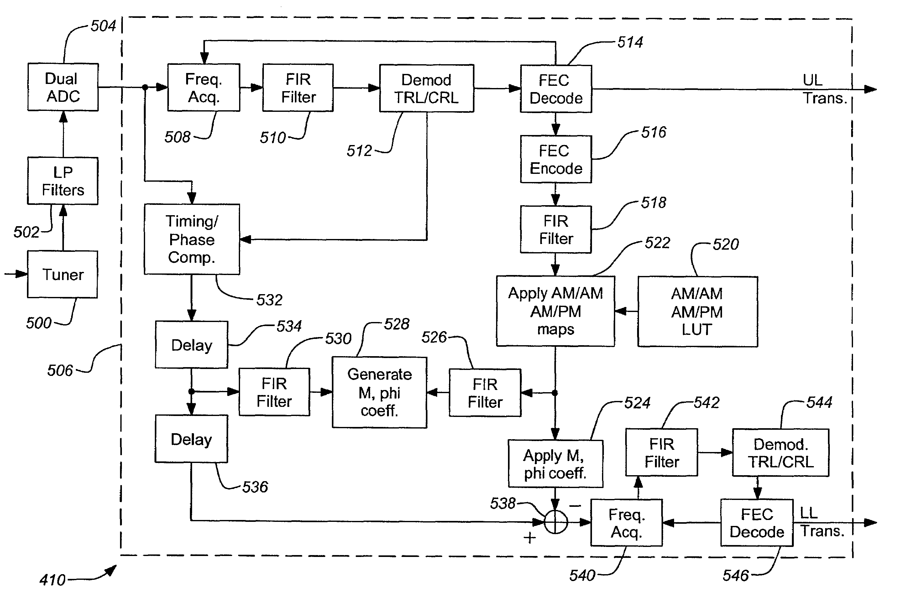
[0028]The present invention provides for the reception of non-coherent layered modulation signals using legacy and multi-layer receivers. The signal layers can be independently modulated and coded. The layered signal is passed through a high speed digitizer to prepare it for digital processing. Processing the digitized layered signal yields the distinct layer signals which can then be presented to separate transports for conversion to a video signal.

[0029]2. Layered Signals

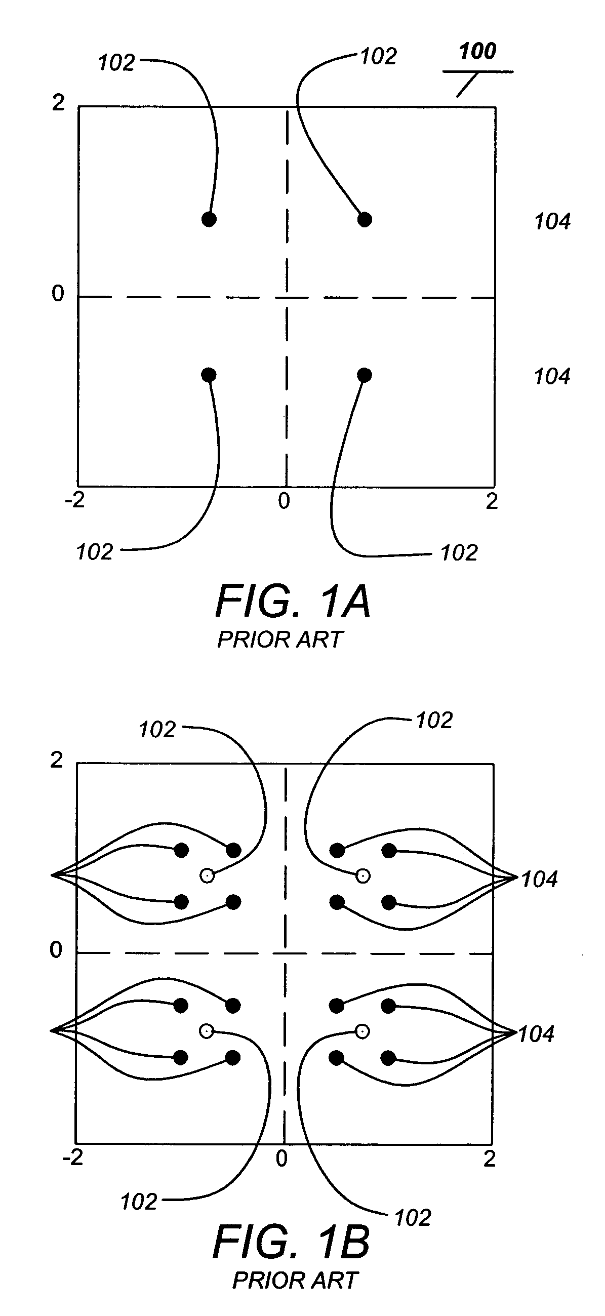
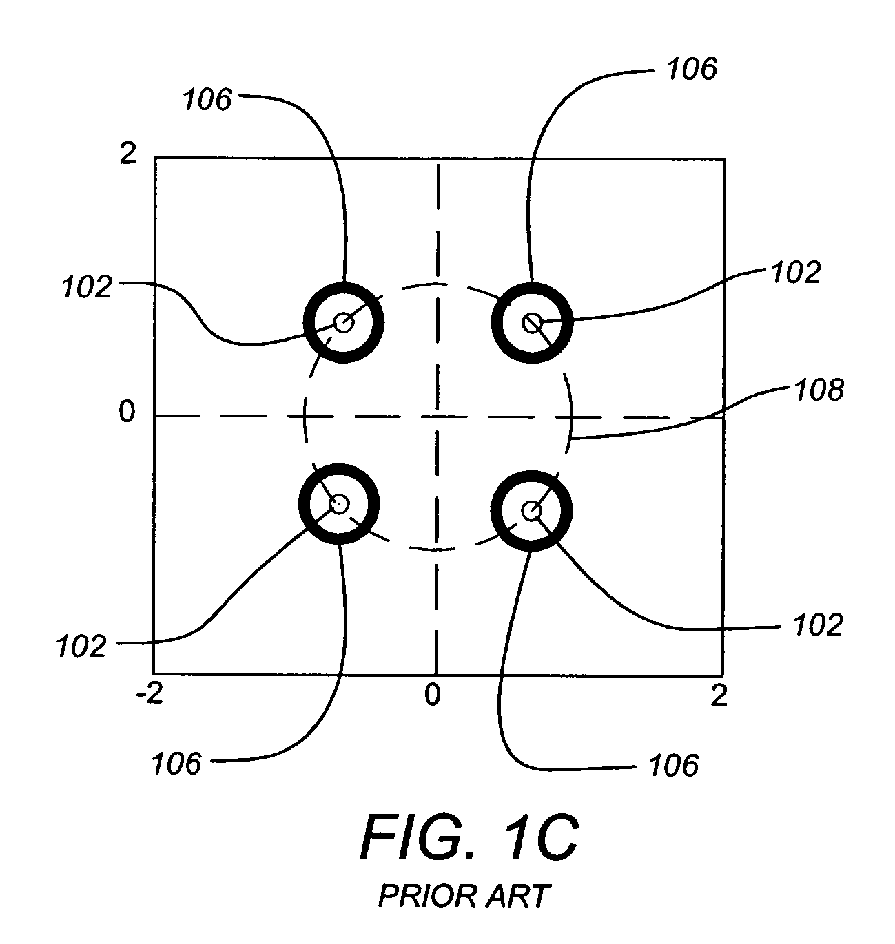
[0030]FIGS. 1A–1C illustrate the basic relationship of signal layers in a layered modulation transmission. FIG. 1A illustrates a upper layer signal constellation 10...


PUM


Abstract

Systems and methods for receiving layered modulation for digital signals are presented. An exemplary apparatus comprises a tuner for receiving a layered signal and producing a layered in-phase signal and a layered quadrature signal therefrom, an analog-to-digital converter for digitizing the layered in-phase signal and the layered quadrature signal and a processor for decoding the layered in-phase signal and the layered quadrature signal to produce one or more discrete layer signals.

Description

CROSS-REFERENCE TO RELATED APPLICATIONS[0001]This is a continuation-in-part application and claims the benefit under 35 U.S.C. Section 120 of the following co-pending and commonly-assigned U.S. utility patent application, which is incorporated by reference herein:[0002]Utility application Ser. No. 09 / 844,401, filed Apr. 27, 2001, by Ernest C. Chen, entitled “LAYERED MODULATION FOR DIGITAL SIGNALS,”.[0003]This application is related to the following co-pending and commonly-assigned U.S. patent applications, which is incorporated by reference herein:[0004]Application Ser. No. 10 / 068,039, filed on the same date herewith, by Ernest C. Chen et al., entitled “PREPROCESSING SIGNAL LAYERS IN A LAYERED MODULATION DIGITAL SIGNAL SYSTEM TO USE LEGACY RECEIVERS,”.BACKGROUND OF THE INVENTION[0005]1. Field of the Invention[0006]The present invention relates generally to systems for receiving digital signals, and in particular, to systems for receiving layered modulation in digital signals.[0007]2...

Claims


Application Information

Patent Timeline
Patent Type & Authority Patents(United States)
IPC IPC(8): H03D3/00H03K9/06H04L27/38H04H20/30H04H40/90H04L27/34H04N5/44
CPCH04H20/30H04H40/90H04L27/3488H04N21/4382H04N5/455H04N21/234327H04N5/4401H04N21/426
Inventor CHEN, ERNEST C.FURUYA, TIFFANY S.HILMES, PHILIP R.SANTORU, JOSEPH
Owner HUGHES ELECTRONICS
Why Eureka
Try Eureka