Method for fabrication of a contact structure

a technology of contact structure and fabrication method, which is applied in the direction of semiconductor devices, semiconductor/solid-state device details, electrical apparatus, etc., can solve the problems of increasing electronic performance requirements, affecting the production efficiency of contact structures, and causing problems relating to electrical conta

Active Publication Date: 2007-02-13
INFINEON TECH AG
View PDF17 Cites 41 Cited by
  • Summary
  • Abstract
  • Description
  • Claims
  • Application Information

AI Technical Summary

Benefits of technology

[0016]The favorable edge coverage of the layer also enables closed coating even of deep openings in a substrate having an electrically conductive layer. The layer comprising tungsten may be used as a current-carrying layer in electroplating, whereby the demands placed upon the seed layer are kept small In particular, the seed layer may have a very small thickness, even traces of copper deposited onto the layer comprising tungsten being sufficient for enabling high-quality electroplating. In particular, due to the high degree of homogeneity and high quality of the layer comprising tungsten, a homogeneous current supply is possible in electroplating, which has advantageous effects on the production of the contact structure which may be produced with a high degree of uniformity and small-scale mechanical interferences. The use of the inventive W layer, which takes on the property of a conducting layer, which is required for electrolytical copper deposition, disposes with the need to have to achieve, with a sputtered copper layer, a conductive connection to the interior of the substrate via.
[0017]The inventive method is particularly advantageous for producing electrical contacts on structured surfaces of semiconductor substrates, and, in particular, of silicon substrates for current and future requirements associated with semiconductor technology. In particular, the inventive method enables, in such applications, a complete filling-up of a deep opening or a deep via hole in a semiconductor substrate, the via hole having a high aspect ratio, for

Problems solved by technology

In many fields there are considerable challenges to producing contact structures due to the increasing demands placed on them in terms of quality and size.
Especially for semiconductor substrates, problems concerning electrical contact arise due to the strong increase in electronic performance requirements.
An impedance of this magnitude being present in the emitter and / or source path of an RF amplifier circuit greatly reduces the gain available.
Even though multiple bonds are of assistance to a certain degree, they still do not, in principle, provide a solution.
In silicon technology, a number of process related difficulties, in particular the low etching rates of silicon, have prevented an introduction of such substrate via contacts.
This technology, however, has the disadvantage of a relatively poor heat dissipation.
With small components, such as discrete transistors and MMICs (MMIC=monolithic microwave IC), an added disadvantage is that a larger die size of silicon is required because of the bumps, and that, at least up to now, no flip-chip bonding process exists that would even so much as get close to the cycle times of “upright” die-bonding.
It has been known in the art to create vias wherein a reverse-side photolithography process and further reverse-side process steps are required, which is an extremely difficult task to perform on thin wafers.
In the above-described patent applications and according to the current state of the art, however, it is practically impossible to fully fill Via holes, which have dimensions of a very high aspect ratio of 1:10, to the required depth using conventional metal coating methods.
The details disclosed in the above patent applications therefore are not sufficient so as to be able to advantageously produce substrate vias.
In addition, the above patent applications do not indicate any practical method specifying how the substrate vias may be exposed and connected in a convenient manner from the reverse side once the front side of the wafers has been completed.

Method used


Image

  • Method for fabrication of a contact structure
  • Method for fabrication of a contact structure
  • Method for fabrication of a contact structure

Examples


Embodiment Construction

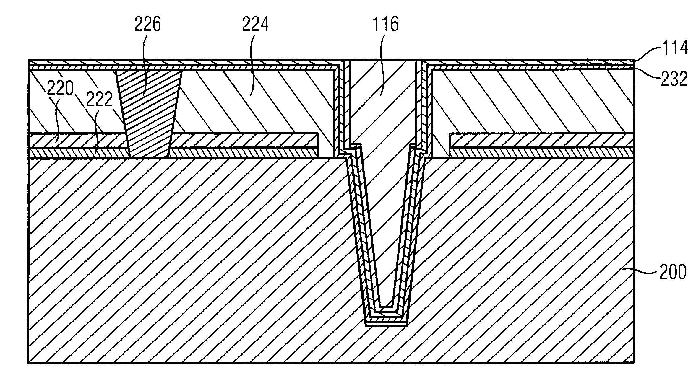
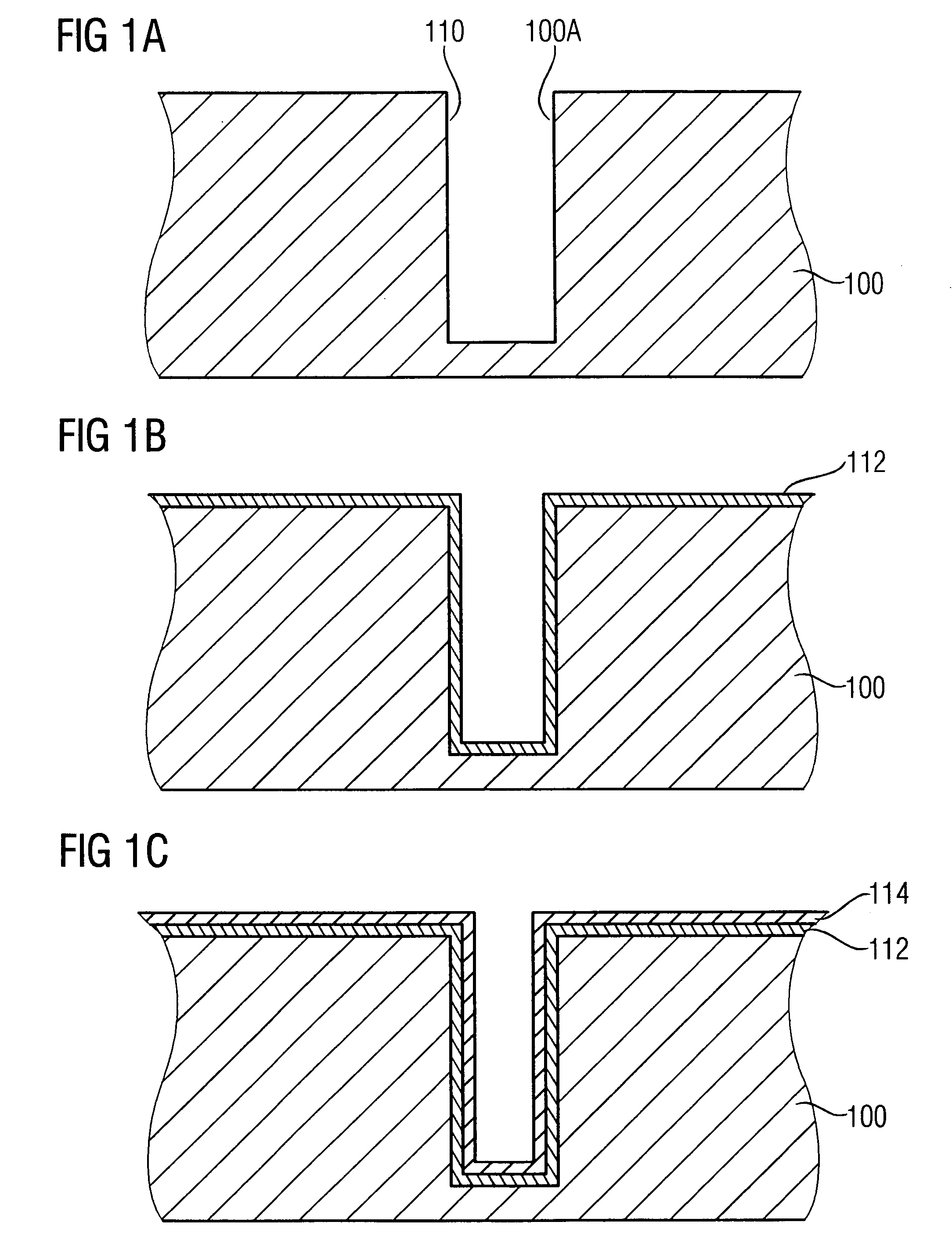
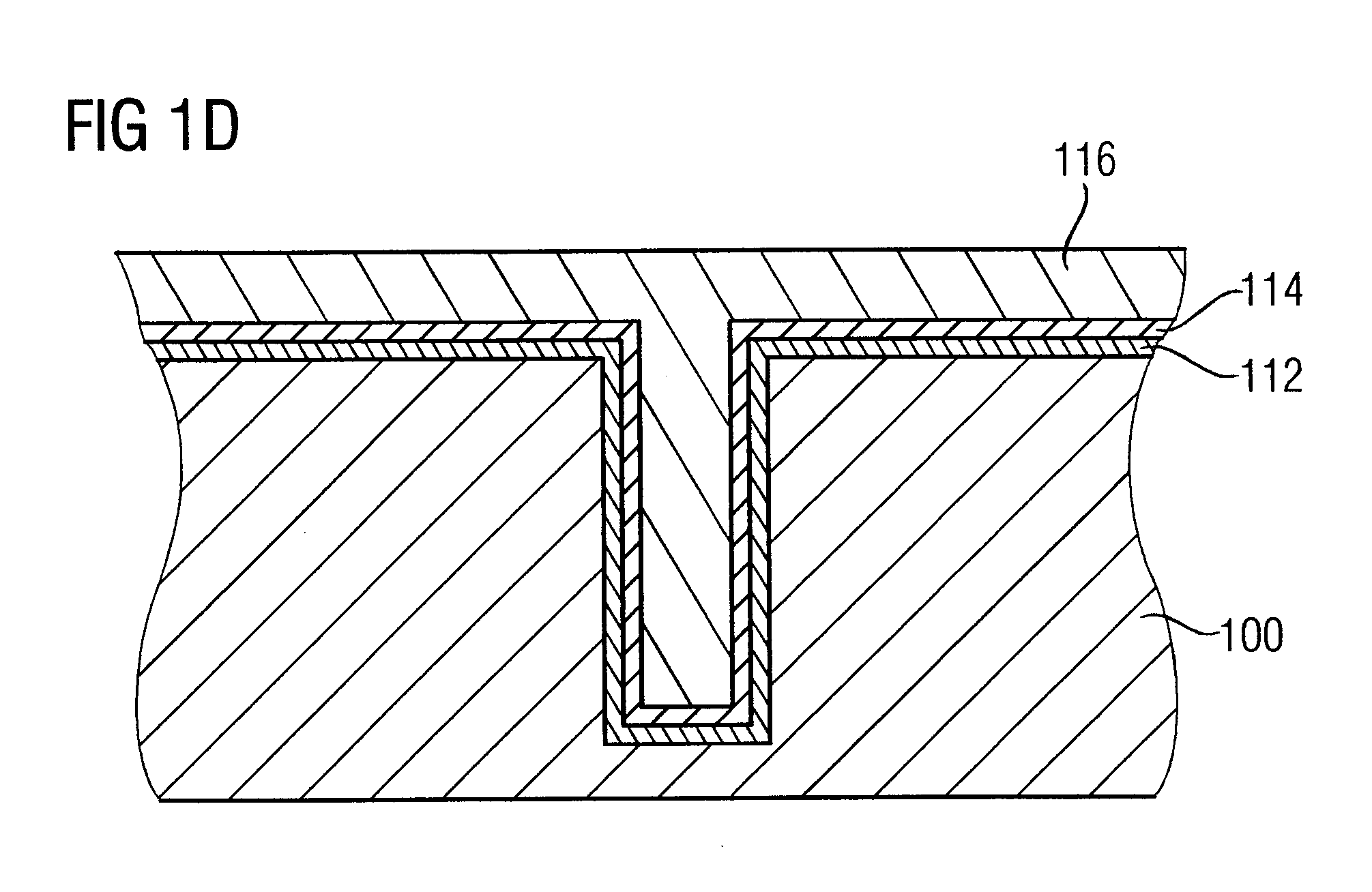
[0030]A first fundamental embodiment of the present invention will be explained below with reference to FIG. 1a–d. In accordance with FIG. 1a, a structured surface 100a is formed in a substrate 100, which surface 100a may be, for example, a surface of a recess or opening 110 in the substrate 100, which opening is filled with an electrically conductive contact. Even though, in the preferred embodiments, a description is merely given of a production of contacts in via holes of a substrate, the present invention is not limited to such structures but may include, for example, the production of a conductive contact on a projection or on other structured surfaces. Substrate 100 may include any known substrate. Preferably, the present invention is particularly suited for producing contacts in a semiconductor substrate, and, as is particularly preferred, in a silicon semiconductor substrate. Substrate 100 may be integrally formed or may include a multi-layer structure with various layer mat...


PUM

PropertyMeasurementUnit
depthaaaaaaaaaa
frequencyaaaaaaaaaa
inductanceaaaaaaaaaa

Abstract

A method for producing a contact structure on a structured surface comprising producing a first conductive layer on the structured surface, wherein the first conductive layer comprising tungsten. A conductive seed layer is produced on the first conductive layer, the contact structure being produced by electroplating on the seed layer. The first conductive layer serves as an etch stop for selectively removing substrate material from the backside.

Description

BACKGROUND OF THE INVENTION[0001]1. Field of the Invention[0002]The present invention relates to the production of contact structures on a structured surface of a substrate.[0003]2. Description of Related Art[0004]In many fields there are considerable challenges to producing contact structures due to the increasing demands placed on them in terms of quality and size. Especially for semiconductor substrates, problems concerning electrical contact arise due to the strong increase in electronic performance requirements. As the frequency range above 1 GHz is being opened up increasingly for semiconductor applications, the need to optimize the contact of the active components to the RF ground becomes more marked. Hitherto, in Si components, the mass potentials have been bonded from the front of the chips to the ground contacts of the package via bond wires. Such a bond wire has an inductance of typically 0.5 nH, depending on the length. This corresponds to an impedance of 3 Ohm at 1 GHz....

Claims


Application Information

Patent Timeline
Patent Type & Authority Patents(United States)
IPC IPC(8): H01L21/4763H01L21/3205H01L23/52H01L21/768H01L23/48H01L23/498
CPCH01L21/76843H01L21/76846H01L21/76873H01L21/76898H01L23/49827H01L23/481H01L2224/0401H01L2924/3011H01L2224/02372H01L2224/13009
Inventor AHRENS, CARSTENHUBER, JAKOBSEIDEL, UWE
Owner INFINEON TECH AG
Why Eureka
Try Eureka