Method and apparatus for plasma nitridation of gate dielectrics using amplitude modulated radio-frequency energy

a technology of amplitude modulated radio frequency energy and gate dielectric layer, which is applied in the direction of electrical apparatus, semiconductor devices, transistors, etc., can solve the problems of increasing the amount of power consumed by the gate, unsatisfactory effects on gate performance and durability, and increasing the leakage current of the ga

Active Publication Date: 2007-02-20
APPLIED MATERIALS INC
View PDF8 Cites 50 Cited by
  • Summary
  • Abstract
  • Description
  • Claims
  • Application Information

AI Technical Summary

Benefits of technology

[0015]The present invention generally relates to a method and an apparatus of plasma nitridation of a gate dielectric by a smooth-varying modulated power source to diminish the plasma electron temperature spike.

Problems solved by technology

Attempts have been made to reduce the thickness of SiO2 gate dielectrics below 20 Å. However, it has been found that the use of SiO2 gate dielectrics below 20 Å often results in undesirable effects on gate performance and durability.
Also, there is typically an increase in gate leakage current, i.e., tunneling current, with thin dielectrics that increases the amount of power consumed by the gate.
Thin SiO2 gate dielectrics may be susceptible to NMOS hot carrier degradation, in which high energy carriers traveling across the dielectric can damage or destroy the channel.
Thin SiO2 gate dielectrics may also be susceptible to PMOS negative bias temperature instability (NBTI), wherein the threshold voltage or drive current drifts with operation of the gate.
This may result in a gate leakage reduction, due to tunneling during the operation of a FET, at the same EOT as the un-nitrided oxide dielectric.
Such a large plasma potential may cause excessive bombardment of the silicon dioxide layer by nitrogen ions, which can cause damage to the silicon dioxide layer.
The large plasma potential may even result in incorporation of nitrogen into the underlying silicon, which diminishes the advantages of nitrogen incorporation in the gate oxide.

Method used


Image

  • Method and apparatus for plasma nitridation of gate dielectrics using amplitude modulated radio-frequency energy
  • Method and apparatus for plasma nitridation of gate dielectrics using amplitude modulated radio-frequency energy
  • Method and apparatus for plasma nitridation of gate dielectrics using amplitude modulated radio-frequency energy

Examples


Embodiment Construction

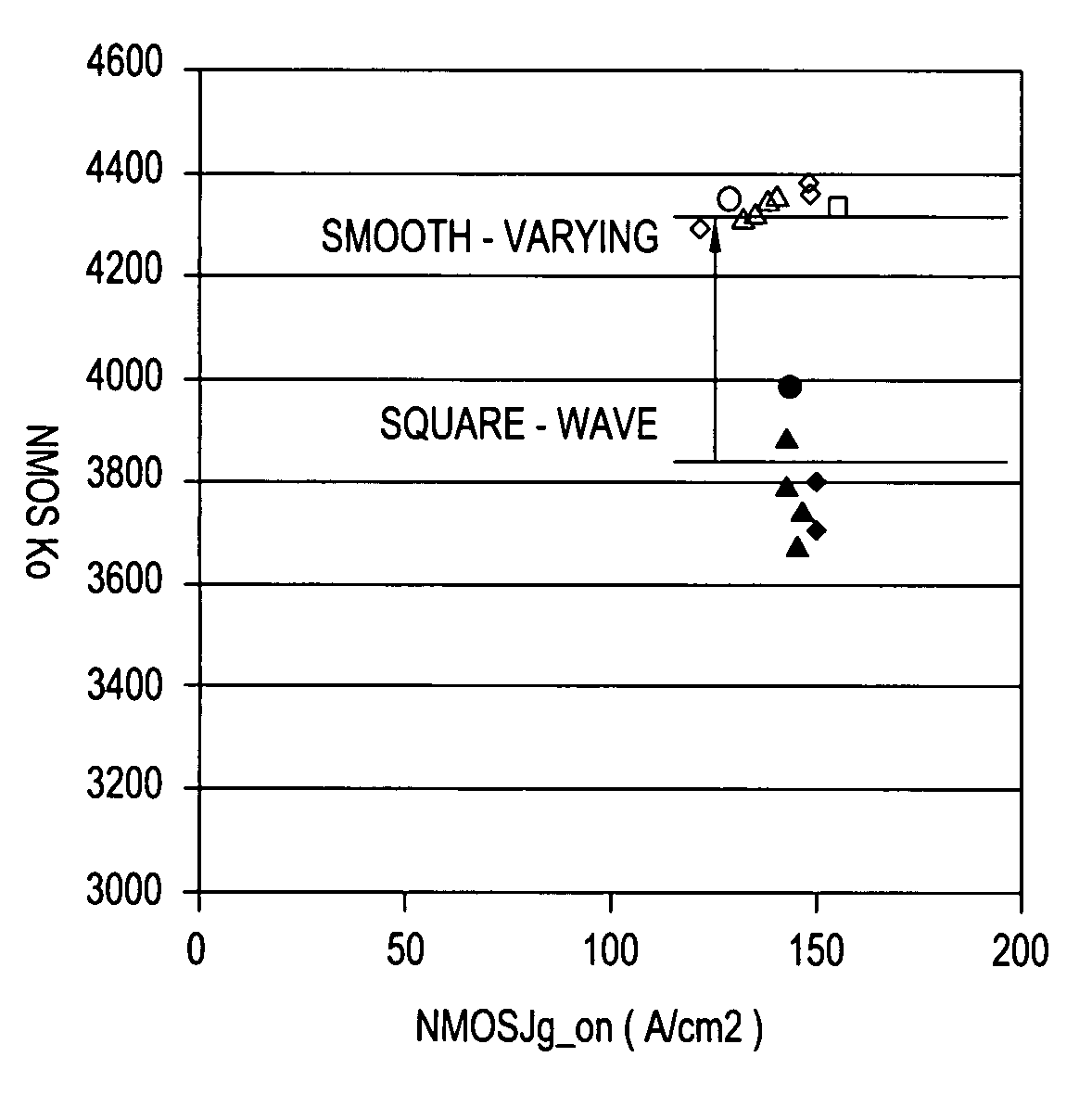
[0038]Embodiments of the invention include a method and an apparatus of plasma nitridation of a gate dielectric. Specifically, the present invention includes a method and an apparatus for diminishing the spike in electron temperature of nitridation plasma through the use of smooth-varying modulated (or pulsed) source power.

[0039]FIG. 3 shows an example of a process flow for plasma nitrided gate dielectrics formation. The process starts with providing a silicon substrate at step 300. First about 5 Å to about 40 Å of a thermal oxide film is grown on a Si wafer at step 302 in either a furnace or a rapid thermal processing chamber. Silicon dioxide (SiO2) gate dielectric is described here as an example. The invention can be applied to other types of gate dielectric, which could be a high-k dielectric material having a dielectric constant greater than 4.0, such as SiON, SiN, hafnium oxide (HfO2), hafnium silicate (HfSiO2), hafnium silicon oxynitride (HfSiON), zirconium oxide (ZrO2), Zirco...


PUM


Abstract

A method and apparatus for forming a nitrided gate dielectric layer. The method includes generating a nitrogen-containing plasma in a processing chamber via a smooth-varying modulated RF power source to reduce electron temperature spike. Field effect transistor channel mobility and gate leakage current results are improved when the power source is smooth-varying modulated, as compared to square-wave modulated.

Description

CROSS-REFERENCE TO RELATED APPLICATIONS[0001]This application claims priority from provisional patent application Ser. No. 60 / 474,125, filed on May 28, 2003, which is herein incorporated by reference.BACKGROUND OF THE INVENTION[0002]1. Field of the Invention[0003]Embodiments of the present invention generally relate to a method and an apparatus of forming a gate dielectric. More particularly, embodiments of the invention relate to a method of forming a nitrided gate dielectric layer.[0004]2. Description of the Related Art[0005]Integrated circuits are composed of many, e.g., millions, of devices such as transistors, capacitors, and resistors. Transistors, such as field effect transistors, typically include a source, a drain, and a gate stack. The gate stack typically includes a substrate, such as a silicon substrate, a gate dielectric, and a gate electrode, such as polycrystalline silicon, on the gate dielectric. The gate dielectric layer is formed of dielectric materials such as sil...

Claims


Application Information

Patent Timeline
Patent Type & Authority Patents(United States)
IPC IPC(8): H01L21/31H01L21/28H01L21/314H01L29/51
CPCH01L21/28202H01L29/518H01L29/517H01L21/3144H01L21/02326H01L21/0234
Inventor KRAUS, PHILIP A.CHUA, THAI CHENG
Owner APPLIED MATERIALS INC
Why Eureka
Try Eureka