Pattern measuring method

a pattern and measurement method technology, applied in the field of pattern measurement method, can solve the problems of instable calculated values, implying extended processing time, and rough edges of patterns, and achieve the effect of stably measuring the width of lines

Active Publication Date: 2007-02-20
HITACHI HIGH-TECH CORP
View PDF5 Cites 5 Cited by
  • Summary
  • Abstract
  • Description
  • Claims
  • Application Information

AI Technical Summary

Benefits of technology

[0010]It is an object of the present invention to provide a measuring method which is capable of stably measuring a line width in a simple manner separately from local roughness.
[0011]Conventional measuring techniques for measuring a line width in a pattern image involve setting a certain target, locally detecting edges within the range of the target, and measuring the line width based on information resulting from the local edge detection, so that the influence of the local edge roughness causes variations in the measured values. The present invention, on the other hand, makes a measurement on an average image of a plurality of the same patterns within the same screen, and can therefore measure the local edge roughness and global roughness, which can cause the variations, and variations in roughness in the screen. Also, when the measurement is specified for the global roughness, the local roughness of an image is averaged by superimposing a plurality of patterns within the same screen, thus reducing errors due to a particular measuring method.

Problems solved by technology

With the increasing miniaturization of semiconductor devices, the edge roughness of a pattern has become a problem.
However, the aforementioned method is adversely affected by the local roughness, so that a line width WA is measured at the measuring position A, while a line width WB is measured at the measuring position B, thus presenting largely differing results of measurement depending on the position set for the measurement.
Also, conventionally, when an average line width is measured for a line or a space pattern image including edge roughness, the line width is locally measured at multiple positions, and measured values are averaged, thus implying problems of an extended processing time, instable calculated values, and the like.

Method used


Image

  • Pattern measuring method
  • Pattern measuring method
  • Pattern measuring method

Examples


Embodiment Construction

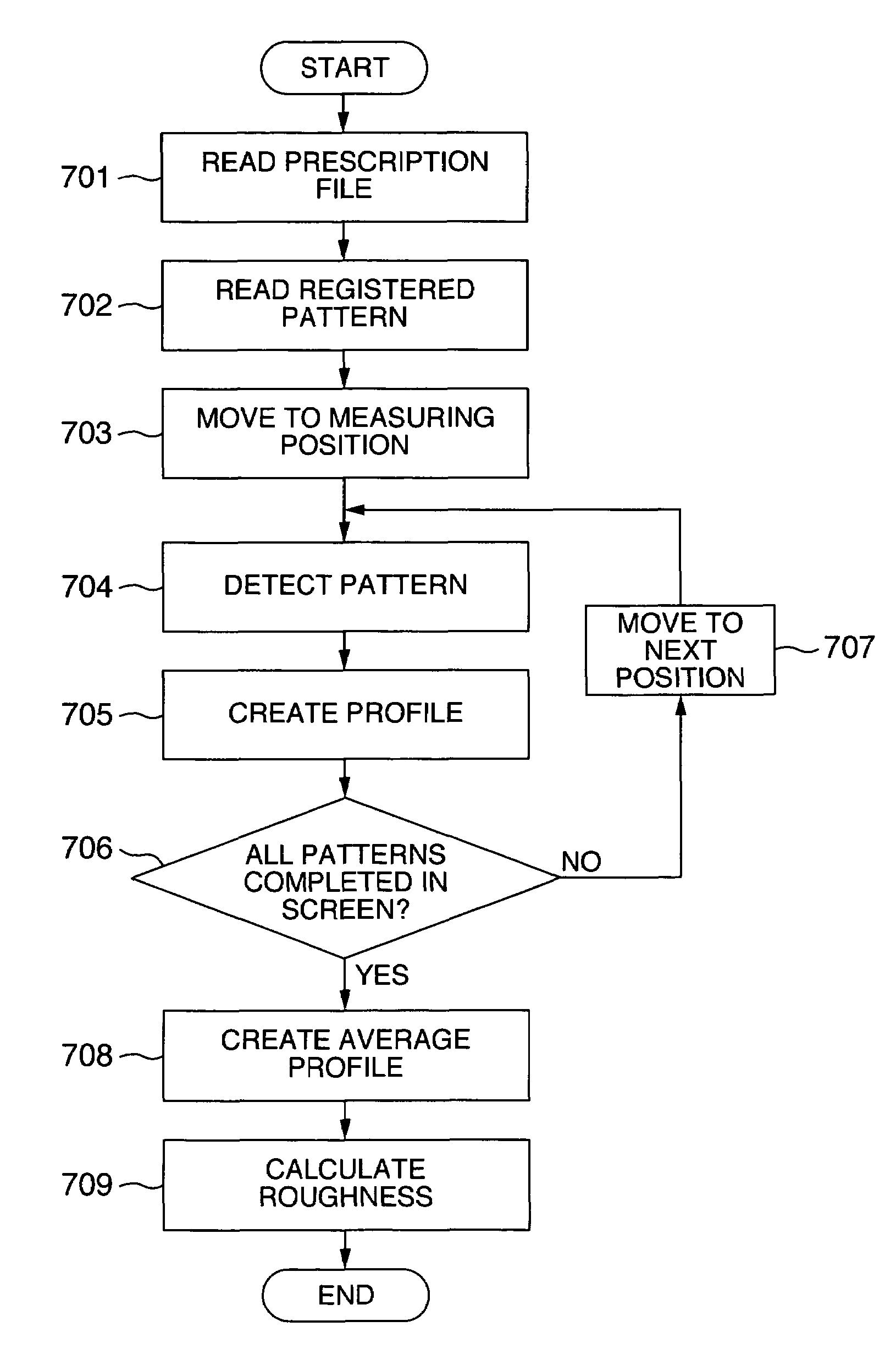
[0024]In the following, one embodiment of the present invention will be described with reference to the accompanying drawings.

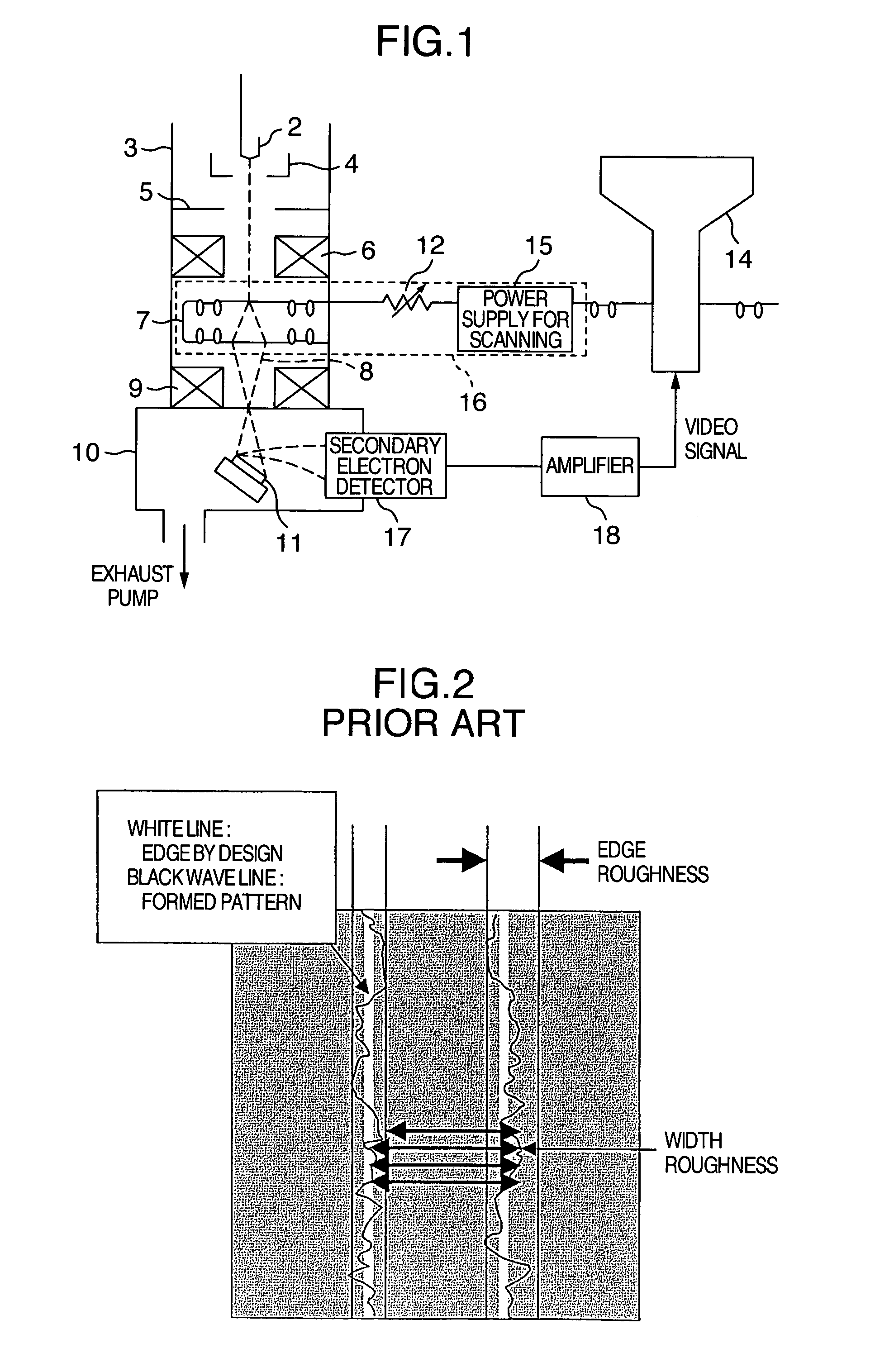
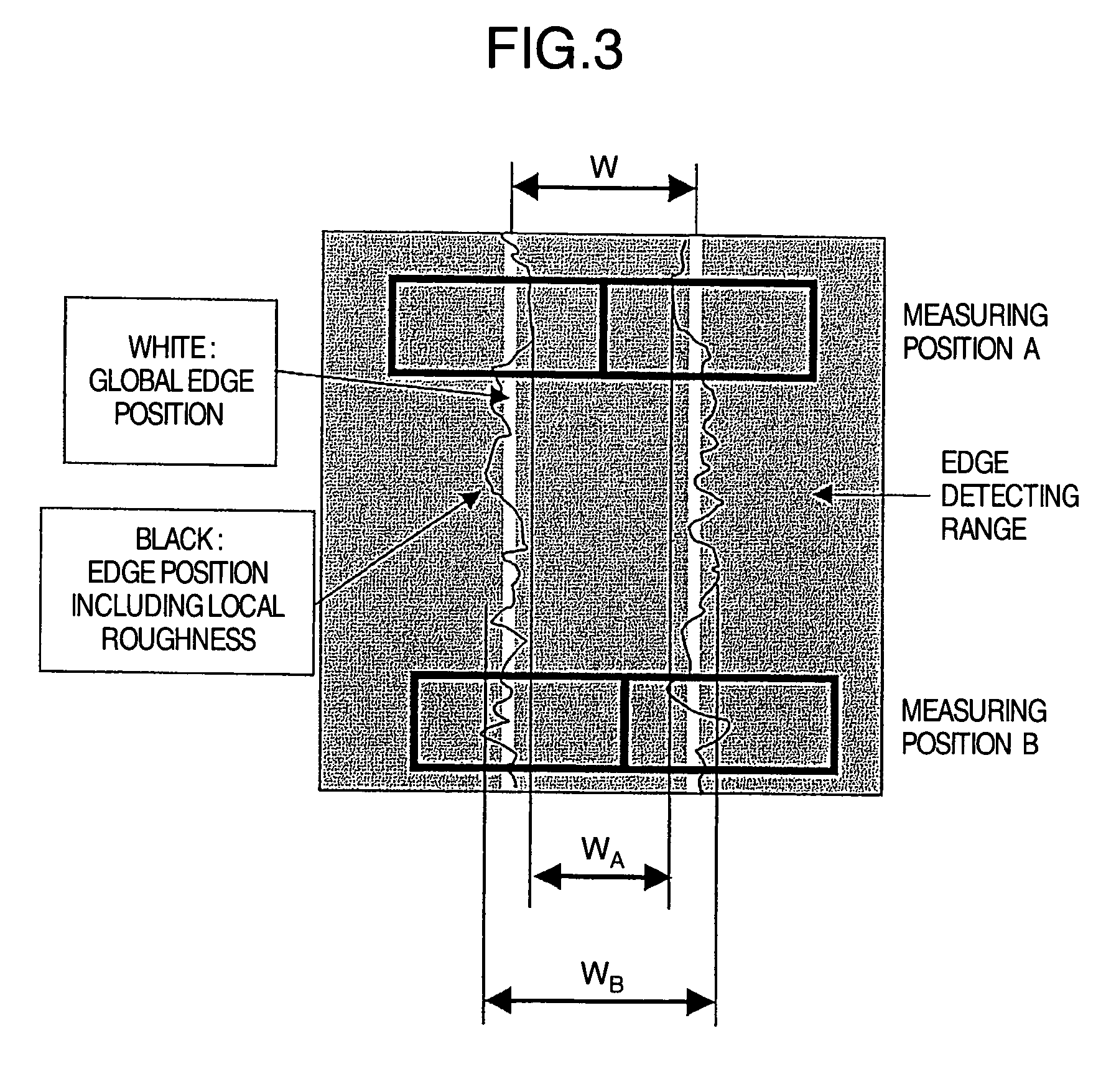
[0025]FIG. 1 is a schematic diagram illustrating an exemplary configuration of a scanning electron microscope for conducting a miniature pattern test according to the present invention. In an electron gun 3, a heating filament 2 is heated with a high voltage (500 volts or higher) to generate an electron beam 8. Subsequently, the electron beam 8 drawn out by a Wehnelt 4 is accelerated by an anode 5. This electron beam 8 is converged by a condenser lens 6, and is scanned in an arbitrary direction by a deflection signal generator 16 which is composed of a deflection coil 7, a scaling factor varying resistor 12, and a scanning power supply 16. Further, the electron beam 8 is focused by an object lens 9, and one-dimensionally or two-dimensionally scanned on a specimen 11 placed in a specimen chamber 10. Miniature patterns are engraved on the specimen 11. The irrad...


PUM

PropertyMeasurementUnit
voltageaaaaaaaaaa
shapeaaaaaaaaaa
scanning electron microscopeaaaaaaaaaa

Abstract

A pattern measuring method calculates an average pattern shape from a plurality of the same patterns appearing within an image captured using an electron microscope, and compares pattern information at each measuring position with average pattern information to determine roughness.

Description

BACKGROUND OF THE INVENTION[0001]The present invention relates to a pattern measuring method for use with a scanning electron microscope which scans a specimen with electron beams and captures information on the surface of the specimen in the form of image from the amount of a secondary electron signal emitted from the specimen as a result of the scanning, and more particularly, to a method of stably measuring an average line width of a pattern.[0002]With the increasing miniaturization of semiconductor devices, the edge roughness of a pattern has become a problem. The edge roughness has been investigated in regard to how it occurs, and attempts have been made for a management based on the roughness value, and a management based on an average measured value including the edge roughness used as an indicator.[0003]FIG. 2 shows an example of a conventional line width measuring method. An edge detecting range is set for a pattern under measurement. The profile of an image is created from...

Claims


Application Information

Patent Timeline
Patent Type & Authority Patents(United States)
IPC IPC(8): H01J31/49G01B15/00G01N23/00G01N23/225G21K7/00H01J37/28
CPCG01N23/225G03F7/70625H01J37/28H01J37/222H01J2237/2814H01J2237/24578
Inventor SASAJIMA, FUMIHIROKIMURA, YOSHIHIROKOMURO, OSAMU
Owner HITACHI HIGH-TECH CORP
Why Eureka
Try Eureka