Electrode line structure having fine line width and method of forming the same

Inactive Publication Date: 2007-02-20
SAMSUNG ELECTRONICS CO LTD
View PDF1 Cites 4 Cited by
  • Summary
  • Abstract
  • Description
  • Claims
  • Application Information

AI Technical Summary

Benefits of technology

[0014]The present invention provides an electrode line structure capable of preventing electrode lines of a semiconductor device from becoming partially removed.

Problems solved by technology

However, as the integration density of the semiconductor devices increases exponentially, it is desirous for the word lines and the bit lines to have a line width not larger than the exposure limit, which results in the following problems.
A line defect is therefore generated in the semiconductor device due to the removal of a large portion of the word lines 20.

Method used


Image

  • Electrode line structure having fine line width and method of forming the same
  • Electrode line structure having fine line width and method of forming the same
  • Electrode line structure having fine line width and method of forming the same

Examples


embodiment 2

[0034](Embodiment 2)

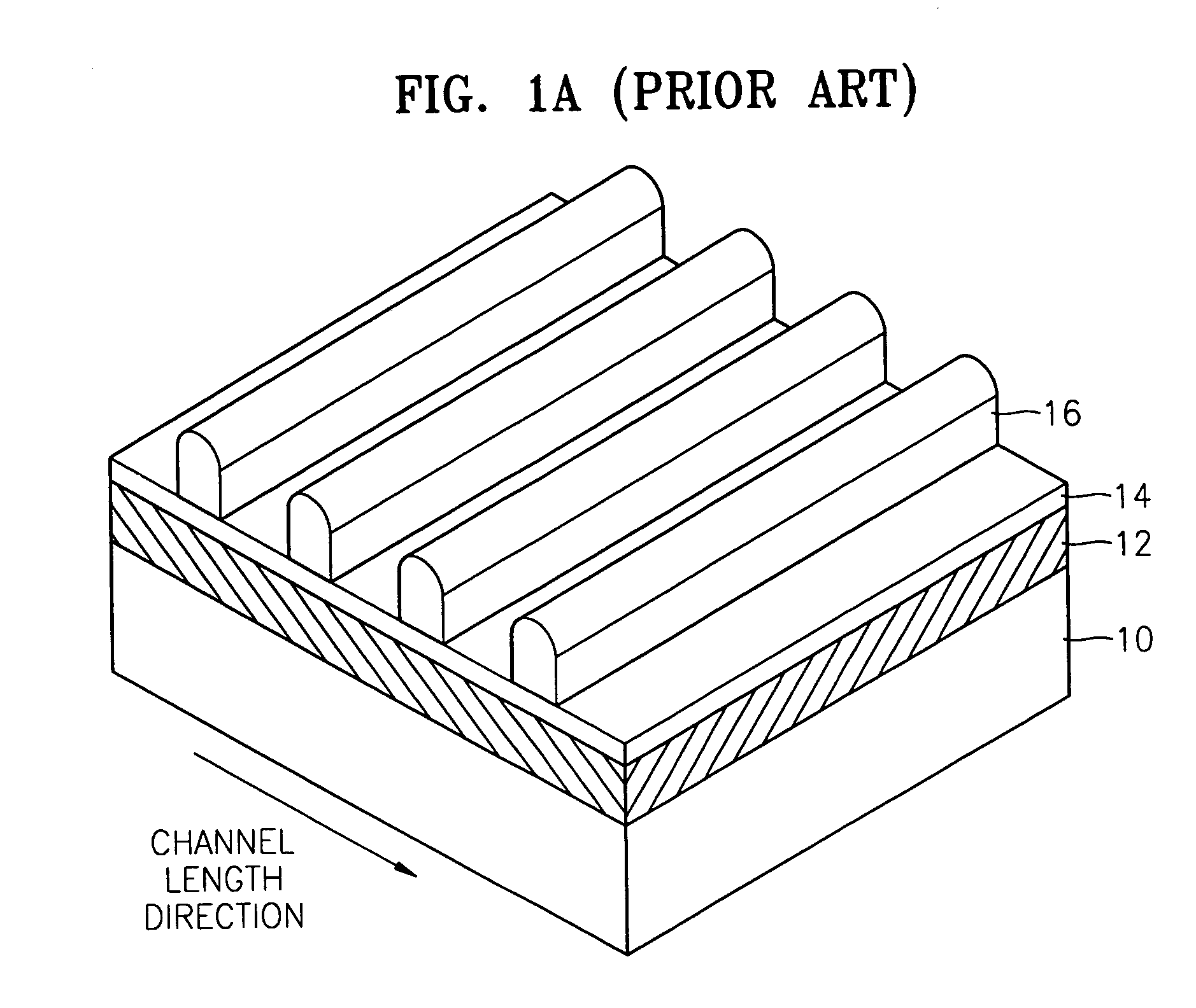
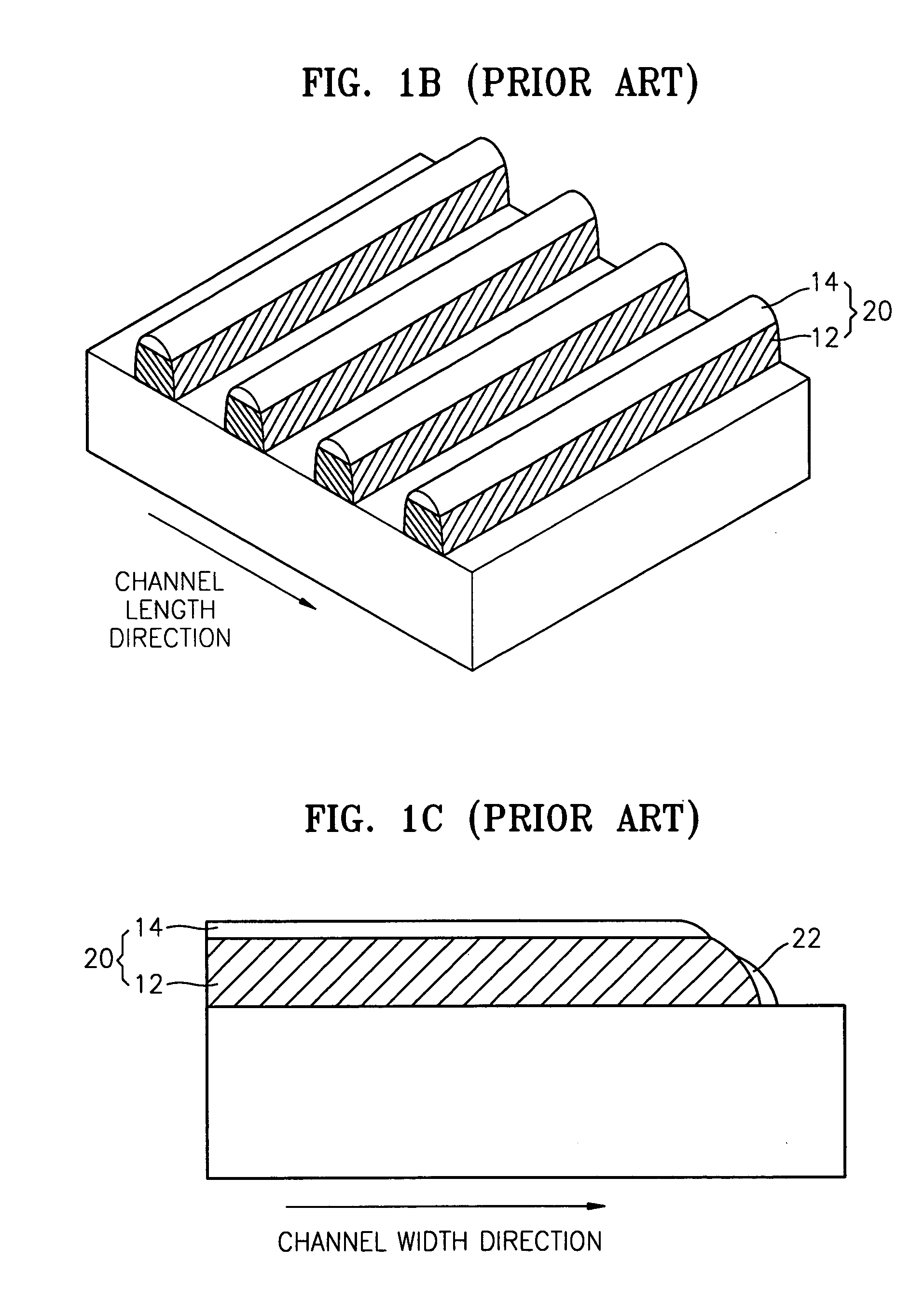
[0035]FIGS. 5A to 5C are cross-sectional views showing a method of forming an electrode line structure of a semiconductor device according to a second embodiment of the present invention. In the present embodiment, the electrode lines are used as word lines.

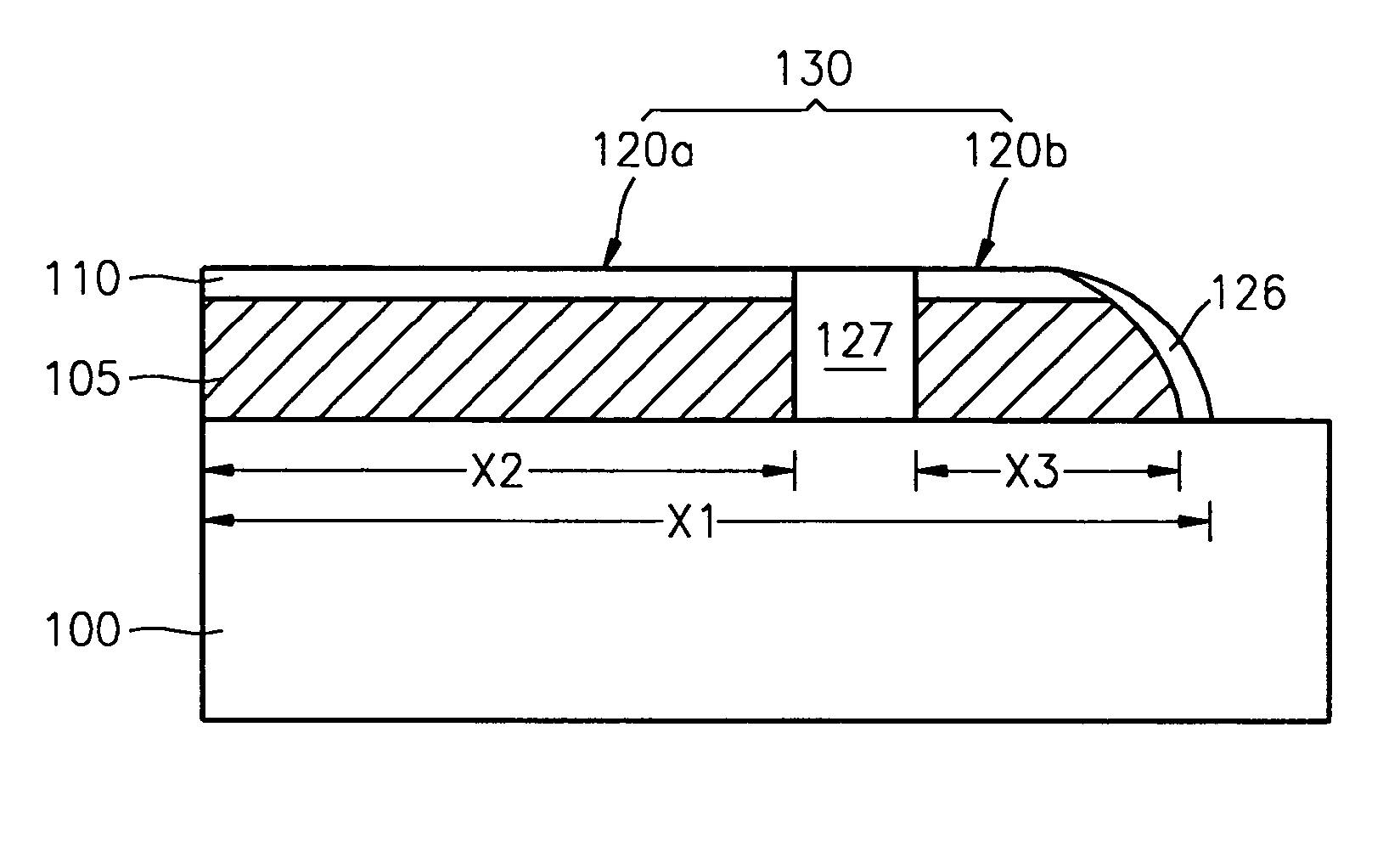
[0036]Referring to FIG. 5A, a conductive layer 105 for word lines is formed on an upper portion of a semiconductor substrate 100. A gate insulating layer (not shown) is formed between the semiconductor substrate 100 and the conductive layer 105. A tungsten metal layer or a tungsten silicide layer may be used as the conductive layer 105. A hard mask layer 110 is formed on an upper portion of the conductive layer 105. The hard mask layer 110 electrically protects the word lines during a subsequent step of forming a self-aligning contact, and may be formed of a silicon nitride layer or a silicon oxynitride layer. Thereafter, photoresist patterns 115 are formed by a known photolithography process in order to defin...


PUM


Abstract

In an electrode line structure of a semiconductor device and a method for forming the same, the electrode line structure comprises a semiconductor substrate, and electrode lines, which are formed on the semiconductor substrate, and have an inclined end in the long axis direction. The electrode lines each include a first line unit, which substantially functions as an electrode line, a second line unit, which has an inclined end in the long axis direction and is separated from the first line unit by a predetermined distance, and an insulating plug, which is interposed between the first line unit and the second line unit and electrically insulates the first line unit from the second line unit.

Description

BACKGROUND OF THE INVENTION[0001]This application claims the priority of Korean Patent Application No. 2002-57462 filed on Sep. 19, 2002, in the Korean Intellectual Property Office, the disclosure of which is incorporated herein in its entirety by reference.[0002]1. Field of the Invention[0003]The present invention relates to a semiconductor device and a method of manufacturing the same, and more particularly, to an electrode line structure having a fine line width and a method of forming the same.[0004]2. Description of the Related Art[0005]As the integration density of semiconductor devices increases, fine circuit patterns having a fine line width or electrode lines having a fine line width are required. In particular, electrode lines such as word lines or bit lines are of the most widely used lines in a DRAM (dynamic random access memory) device, and the line width of the electrode lines is considered to be the barometer of the level of integration and performance of the highly-i...

Claims


Application Information

Patent Timeline
IPC IPC(8): H01L23/48H01L27/108H01L21/28H01L21/3213H01L21/8242H01L23/528
CPCH01L23/5283H01L27/10888H01L27/10891H01L2924/0002H01L2924/00H10B12/488H10B12/485H01L21/28
Inventor LEE, JOO-WONCHU, KANG-SOOPARK, JAE-EUNYANG, JONG-HO
Owner SAMSUNG ELECTRONICS CO LTD
Why Eureka
Try Eureka