
Series diode thermally assisted MRAM

a diode and thermal assisted technology, applied in the field of information storage devices, can solve the problems of increasing the burden of error code correction, non-selective heating, and inability to use external heaters in many applications,

Active Publication Date: 2007-02-20
SAMSUNG ELECTRONICS CO LTD
View PDF12 Cites 73 Cited by
  • Summary
  • Abstract
  • Description
  • Claims
  • Application Information

AI Technical Summary

Benefits of technology

This approach improves write reliability and efficiency by reducing the coercivity of the magnetic memory elements, allowing for smaller, higher-density devices with lower current usage and selective heating of only the required cells.

Problems solved by technology

In practice, however, the combined magnetic fields do not always flip the magnetization orientation.
If the magnetization orientation of the selected SDT junction is not flipped, a write error is made and an increased burden on error code correction can result.
Problems with this heating method include nonselective heating, including heating components that do not enhance thermal assisted switching and the write process.
An external heater is not practical for many applications, and typically requires very high external temperatures.
Thermal time constants associated with external heating also tend to be relatively long, resulting in slow overall operation of the device.
However, the magnitude of the power generated from self-heating is generally insufficient to enhance the write operation in any material way.

Method used


Image

  • Series diode thermally assisted MRAM
  • Series diode thermally assisted MRAM
  • Series diode thermally assisted MRAM

Examples


Embodiment Construction

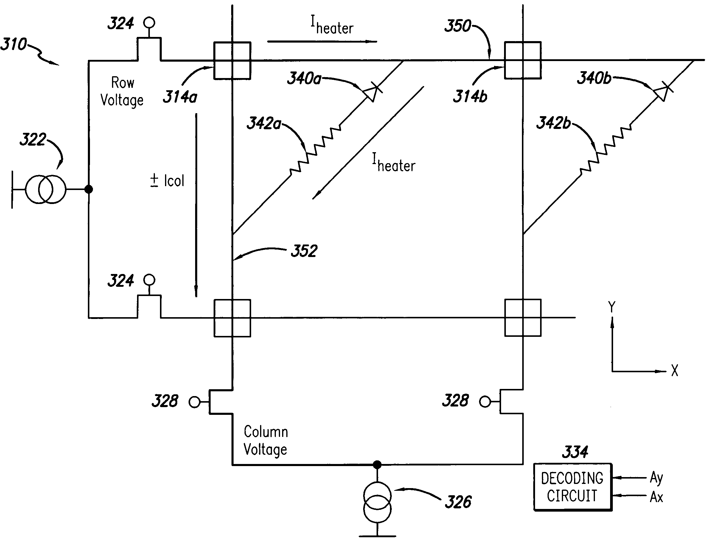
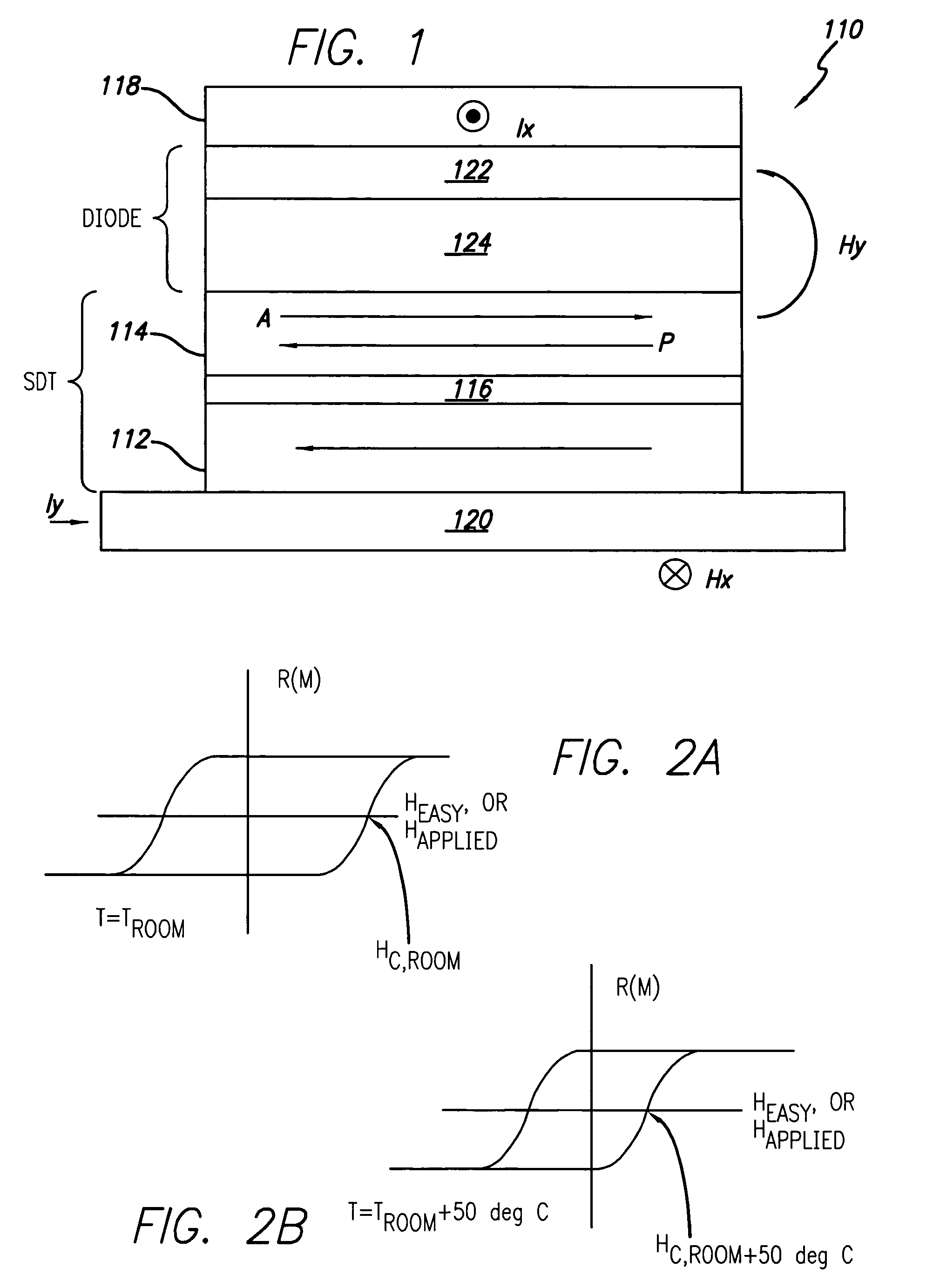
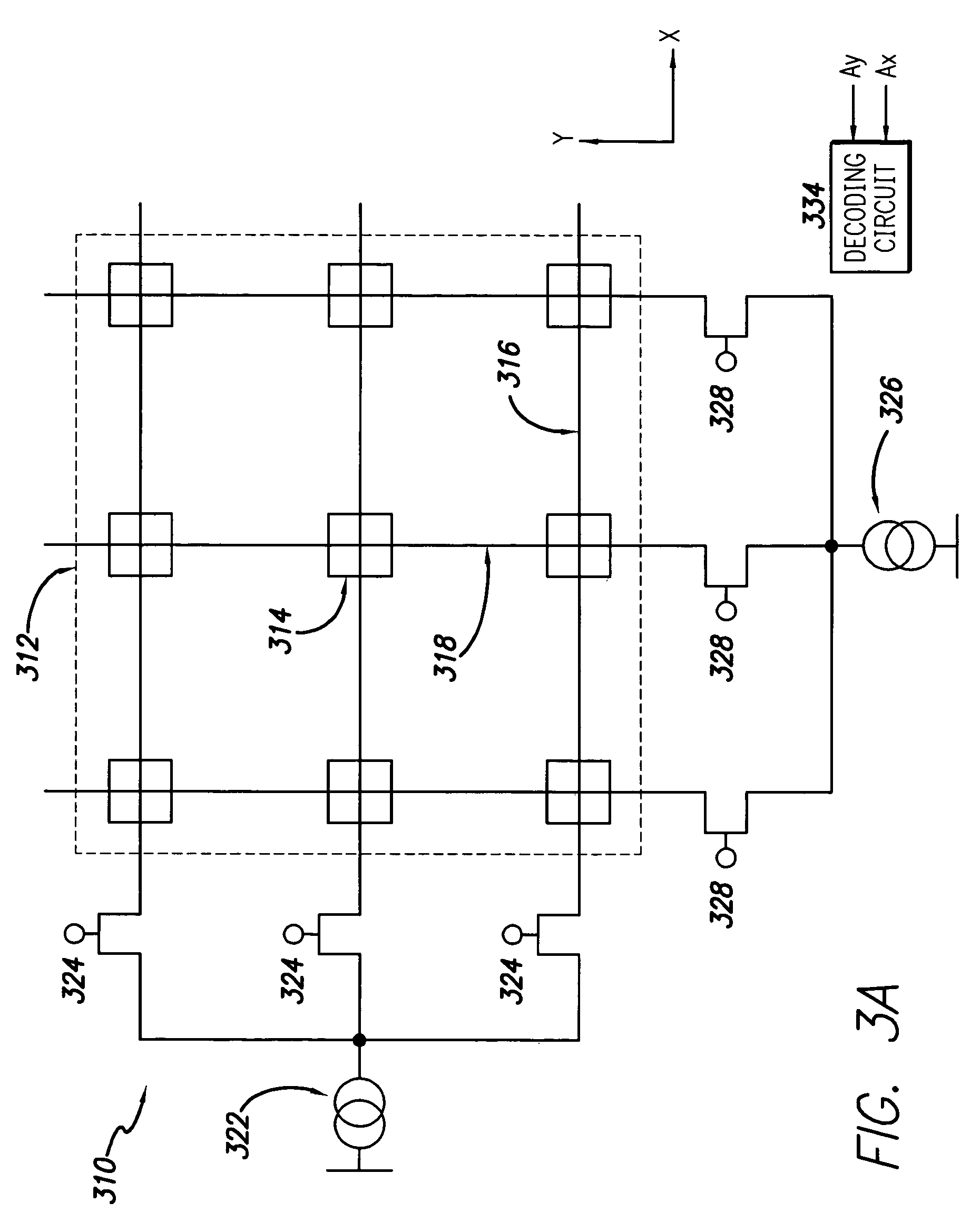
[0021]The present invention is a series diode thermally assisted MRAM device formed by integrating a thin film junction diode in series with a tunnel junction MRAM memory cell. During data storage, the MRAM device performs thermally assisted switching of selected memory elements using thin film junction diodes connected to the SDT junction in series. Thermally assisted switching using a thin film junction diode in series with a tunnel junction MRAM memory cell improves the reliability data storage in the MRAM device. Such thermally assisted switching also enables the employment of smaller devices having higher densities and using lower currents.

[0022]A magnetic memory element of the MRAM device could be any element having a resistance that is dependent upon the state of its magnetic film. Examples of such elements include magnetic tunnel junctions, where the SDT junction is a type of magnetic tunnel junction. Other types of magnetic memory elements include giant magnetoresistance (“...


PUM


Abstract

An information storage device is provided. The information storage device may be a magnetic random access memory (MRAM) device including a resistive cross point array of spin dependent tunneling (SDT) junctions or magnetic memory elements, with word lines extending along rows of the SDT junctions and bit lines extending along the columns of the SDT junctions. The present design includes a plurality of heating elements connected in series with associated magnetic memory elements, each heating element comprising a diode. Voltage applied to a magnetic memory element and associated heating element causes reverse current to flow through the diode, thereby producing heat from the diode and heating the magnetic memory element, thereby facilitating the write function of the device.

Description

BACKGROUND OF THE INVENTION[0001]1. Field of the Invention[0002]The present invention relates generally to the field of information storage devices, and more particularly to the magnetic random access memory (MRAM) devices and thermal properties associated therewith.[0003]2. Description of the Related Art[0004]Magnetic Random Access Memory, or MRAM, is a non-volatile memory that may be employed for both short term and long term data storage. One implementation of an MRAM device includes a resistive cross point array of spin dependent tunneling (SDT) junctions, with word lines extending along rows of the SDT junctions and bit lines extending along the columns of the SDT junctions. Each SDT junction is located at a cross point of a word line and a bit line. The magnetization of each SDT junction assumes one of two stable orientations at any given time. These two stable orientations, parallel and anti-parallel, represent logic values of ‘0’ and ‘1.’ The magnetization orientation, in tu...

Claims


Application Information

Patent Timeline
Patent Type & Authority Patents(United States)
IPC IPC(8): G11C11/02
CPCG11C11/16G11C11/1675
Inventor PERNER, FREDERICK A.NICKEL, JANICETRAN, LUNG
Owner SAMSUNG ELECTRONICS CO LTD
Learn More