Method for fabricating a semiconductor device

a semiconductor and device technology, applied in the field of semiconductor devices, can solve the problems of parasitic capacitance, adhesive property, interconnection delay, etc., and achieve the effects of small hardness, large elastic modulus, and large hardness

Active Publication Date: 2007-02-27
FUJITSU SEMICON LTD
View PDF14 Cites 6 Cited by
  • Summary
  • Abstract
  • Description
  • Claims
  • Application Information

AI Technical Summary

Benefits of technology

[0016]According to the present invention, in a semiconductor device having a multi-layer interconnection structure being a structure in which a second interlayer insulation film with a large hardness and an large elastic modulus is stacked on a first interlayer insulation film with a small hardness and a small elastic modulus, the concentration of tensile stress in the antireflective film and the problem of the generation of a crack caused thereby in the multi-layer interconnection structure can be avoided by forming the antireflective film as a film containing no tensile stress.
[0017]Particularly, the present invention is very useful for suppressing the generation of a crack in a multi-layer interconnection structure in an ultra-fine semiconductor device containing a fine pattern with a small radius of curvature.

Problems solved by technology

On the other hand, a multi-layer interconnection structure is used for interconnecting among respective semiconductor devices in a recent high-density semiconductor integrated circuit device but, with regard to such a multi-layer interconnection structure, when the semiconductor device is very finely miniaturized, interconnection patterns in the multi-layer interconnection structure are close to each other and the problem of an interconnection delay caused by a parasitic capacitance among the interconnection patterns occurs.
Since the low dielectric constant film generally has a small density, there remain problems of the adhesive property with the interconnection pattern, humidity resistance, etc.

Method used


Image

  • Method for fabricating a semiconductor device
  • Method for fabricating a semiconductor device
  • Method for fabricating a semiconductor device

Examples


first embodiment

[0061][The First Embodiment]

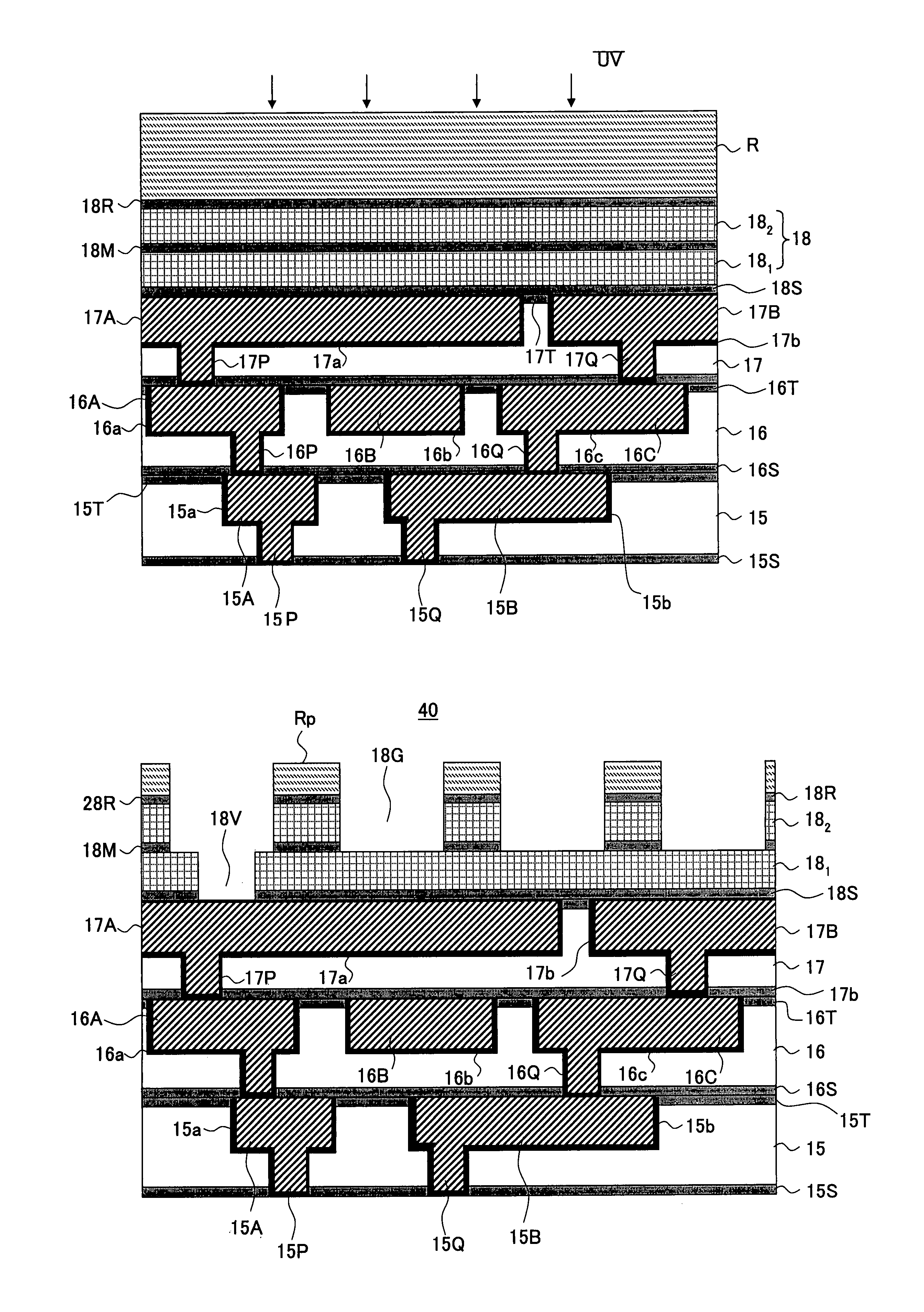
[0062]FIGS. 14–17 indicate a process for fabricating a semiconductor device 40 according to one embodiment of the present invention. Herein, the same reference numeral is assigned to a part corresponding to a previously described part in the figures, the description of which is omitted.

[0063]Referring to FIG. 14, the SiN antireflective film 18R that stores strong tensile stress is replaced by a SiN antireflective film 28R that stores compressive stress or no stress in the present embodiment.

[0064]A process for forming the SiN antireflective film 28R is described below.

[0065]In the present embodiment, the multi-layer structure illustrated in FIG. 2 is introduced into a plasma CVD apparatus 50 illustrated in FIG. 18 before the resist film R is formed, then a Si material gas such as silane and a nitrogen-containing gas such as NH3 are fed, and the SiN antireflective film 28R is formed on the SiOC interlayer insulation film 18 on the condition of storing no t...

second embodiment

[0085][The Second Embodiment]

[0086]In the aforementioned embodiment, a SiN film having compressive stress or no stress as the antireflective film 28R and having a refractive index n and an attenuation constant k being a proper value for an antireflective film is used but the present invention is not limited to a SiN antireflective film and can be applied to, for example, a SiON antireflective film.

[0087]Although the SiON film has tensile stress on the order of 200 MPa when formed by means of the normal plasma CVD method, a formed SiON film is made to be a no-stress film or a compressive stress film by using He for a plasma gas in the present embodiment.

[0088]The condition of forming such a SiON antireflective film is shown in the following table 3.

[0089]

TABLE 3SiH4 = 55 SCCMN2O = 105 SCCMHe =2000 SCCMGap = 370 milsRF = 110 WProcess pressure =  5.5 TorrTemp. =350° C.

[0090]Herein, “Gap” in table 3 indicates a distance between the substrate to be processed 52 and the shower head 53 in ...


PUM


Abstract

A semiconductor device has a multi-layer interconnection structure with a first interlayer insulation film and a second interlayer insulation film that is formed on the first interlayer insulation film and has a hardness and an elastic modulus larger than those of the first interlayer insulation film, and is fabricated by a step of forming a resist film on the second interlayer insulation film via an antireflective film, a step of exposing to light and developing the resist film to form a resist pattern, and a step of patterning the antireflective film and the multi-layer interconnection structure using the resist pattern as a mask, wherein a film with no stress or for storing compressive stress is used as the antireflective film.

Description

CROSS-REFERENCE TO RELATED APPLICATIONS[0001]The present application is a U.S. continuation application filed under 35 U.S.C. 111(a) claiming benefit under 35 U.S.C. 120 and 365(c) of International Patent Application No. PCT / JP03 / 05458 filed on Apr. 28, 2003, the entire contents of which are hereby incorporated by reference.BACKGROUND OF THE INVENTION[0002]1. Field of the Invention[0003]The present invention relates generally to a semiconductor device and, particularly, to a method for fabricating a semiconductor device having a multi-layer interconnection structure.[0004]2. Description of the Related Art[0005]Conventionally, an effort for speeding up of a working speed according to a scaling law has been made by finely miniaturizing a semiconductor device. On the other hand, a multi-layer interconnection structure is used for interconnecting among respective semiconductor devices in a recent high-density semiconductor integrated circuit device but, with regard to such a multi-layer...

Claims


Application Information

Patent Timeline
Patent Type & Authority Patents(United States)
IPC IPC(8): H01L21/4763H01L23/52H01L21/768H01L23/532
CPCH01L21/76829H01L21/76835H01L23/53238H01L21/76807H01L2924/0002H01L2924/3011H01L2924/00
Inventor INOUE, KENGO
Owner FUJITSU SEMICON LTD
Why Eureka
Try Eureka