Passivation structure with voltage equalizing loops

a voltage equalizing loop and passivation structure technology, applied in the direction of semiconductor devices, semiconductor/solid-state device details, electrical apparatus, etc., can solve the problems of increasing the size of the die, affecting the precision of ribbon manufacturing, and not being representative of the intensity of the electric field around the active region. to achieve the effect of reducing the electric field

Active Publication Date: 2007-02-27
INFINEON TECH AMERICAS CORP
View PDF8 Cites 14 Cited by
  • Summary
  • Abstract
  • Description
  • Claims
  • Application Information

AI Technical Summary

Benefits of technology

[0009]It is an object of the present invention to provide a passivation structure to reduce the electric fields around the active region of a semiconductor die.
[0014]According to yet another aspect of the present invention a conductive metallic layer is deposited above at least the PN junctions in the continuous strip to improve (reduce) its RC time constant and to reduce total resistance.

Problems solved by technology

This initial voltage, however, may not be representative of the intensity of the electric field around the active region.
This width could occupy a large area on the surface of the die, thereby increasing the size of the die.
In practice, such a ribbon may be difficult to manufacture with precision.
As a result the resistance along the length of the ribbon may vary in an unpredictable manner leading to fluctuations in the voltage drop rather than a smooth, near linear voltage drop.

Method used


Image

  • Passivation structure with voltage equalizing loops
  • Passivation structure with voltage equalizing loops
  • Passivation structure with voltage equalizing loops

Examples


Embodiment Construction

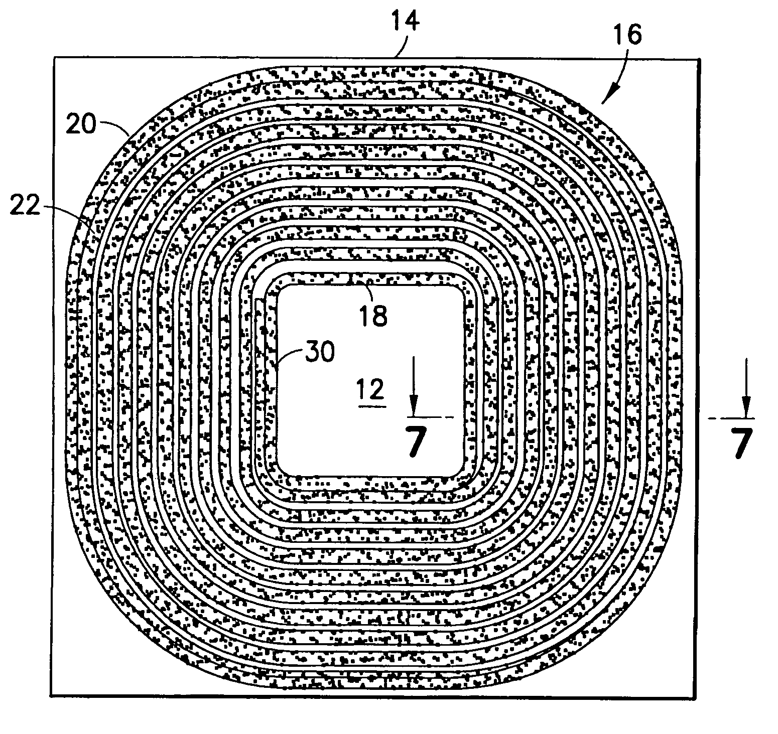
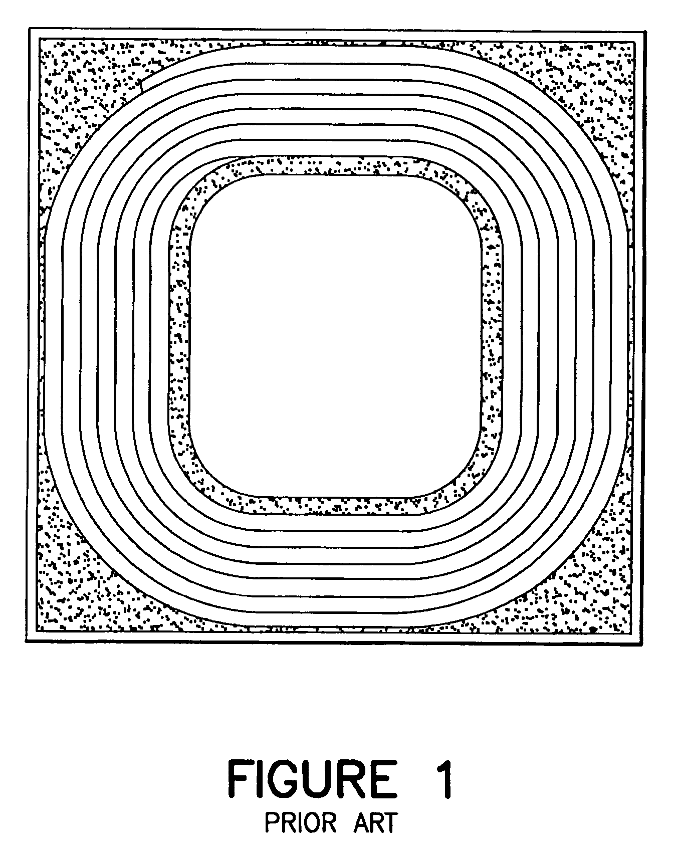
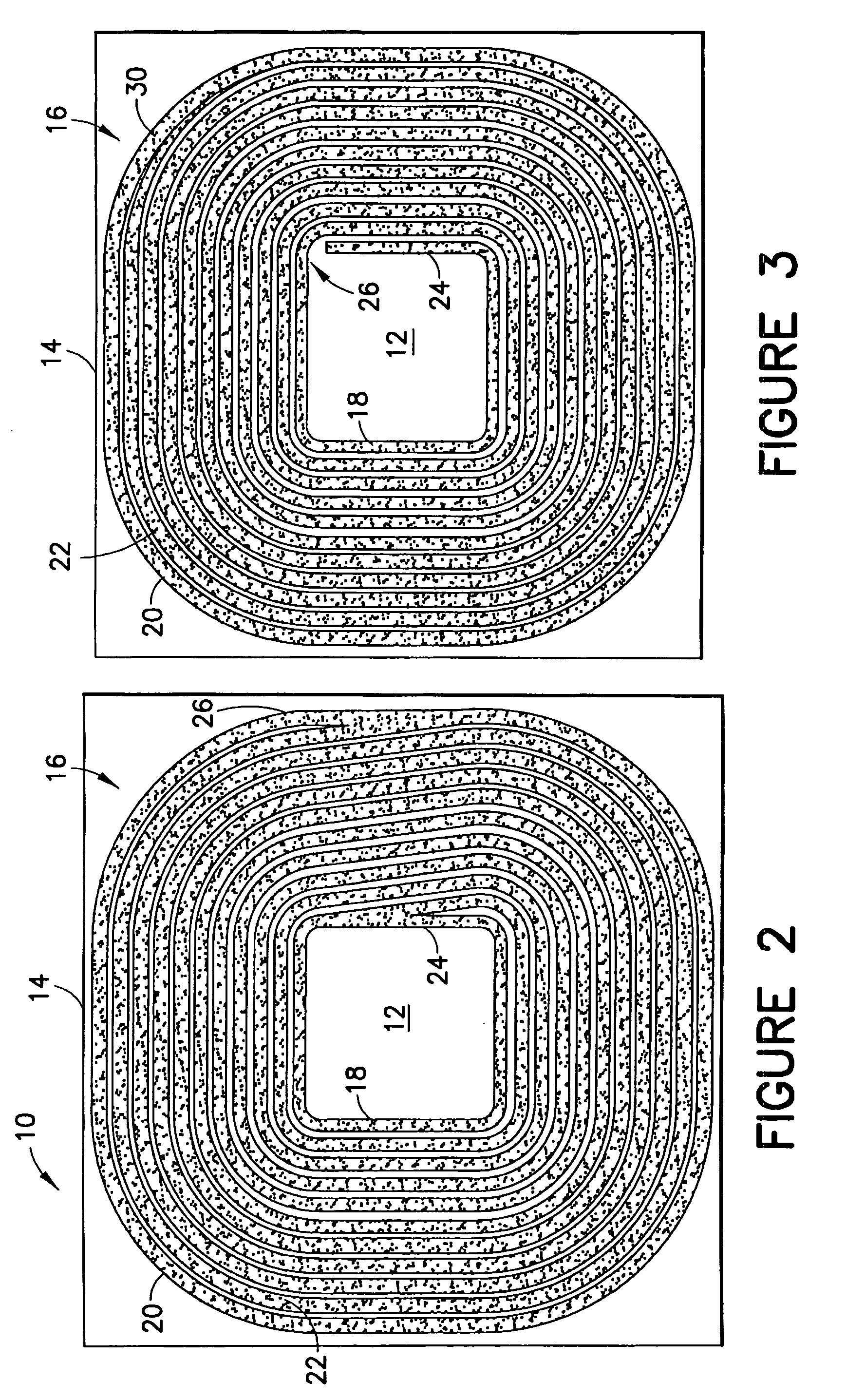
[0023]Referring to FIG. 2, the first embodiment of the present invention is a semiconductor device 10 which includes an active region 12 formed on a major surface of a semiconductor die 14. Active region 12 may include active elements that form a particular semiconductor device such as a power MOSFET, power IGBT, power bipolar device, power diode and so on. Device 10 includes passivation structure 16 formed around active region 12. Passivation structure 16 is formed from a continuous conductive strip of resistive material such as N-type doped polysilicon and includes an inner closed loop 18 which is located immediately around active region 12, and outer closed loop 20 formed around inner closed loop 18 and serving as the outer boundary of passivation structure 16. Inner closed loop 18 has a rectangular shape with rounded corners and thus includes two pairs of parallel straight sides connected to one another by four arcs. The outer closed loop 20 has substantially the same shape as t...


PUM


Abstract

A semiconductor device which includes a passivation structure formed with a conductive strip of resistive material that crosses itself once around the active region of the device to form a first closed loop, a continuous strip that loops around the first closed loop without crossing itself which crosses itself a second time to form a second closed loop.

Description

BACKGROUND OF THE INVENTION[0001]The present invention relates to a semiconductor device and more particularly to a semiconductor device that includes an edge passivation structure.[0002]A typical semiconductor device usually includes an active region which terminates at a PN junction.[0003]The breakdown down voltage of a PN junction formed in a substrate is usually less than its theoretical limit because certain locations on the PN junction have a tendency to develop higher electric fields. The PN junction at the terminal edge of the active region of a device, for example, experiences higher electric fields particularly at locations of low radius of curvature.[0004]To reduce the intensity of the electric fields near the PN junction at the terminal edge of the active region, high voltage semiconductor devices may include an edge passivation structure. An edge passivation structure provides a transition region in which the high electric fields around the active area change gradually ...

Claims


Application Information

Patent Timeline
Patent Type & Authority Patents(United States)
IPC IPC(8): H01L29/00
CPCH01L23/585H01L29/402H01L2924/0002Y10S438/965H01L2924/00H01L29/40H01L29/04H01L27/02H01L29/80
Inventor RANJAN, NIRAJ
Owner INFINEON TECH AMERICAS CORP
Why Eureka
Try Eureka