Manufacture method of VDMOS device with irradiation resistance

A device manufacturing method and anti-irradiation technology, which is applied in semiconductor/solid-state device manufacturing, semiconductor devices, electrical components, etc., can solve the problems of unfavorable anti-single event grid penetration, etc., to improve the anti-single event grid penetration ability and reduce the electric field , The effect of simple process

Active Publication Date: 2015-04-29
BEIJING MXTRONICS CORP +1
View PDF3 Cites 8 Cited by
  • Summary
  • Abstract
  • Description
  • Claims
  • Application Information

AI Technical Summary

Problems solved by technology

However, reducing the thickness of the gate oxide layer will increase the electric field generated by the same amount of holes in the gate dielectric when the device is incident by heavy particles, which is not conducive to the resistance to single event gate breakdown.
The improvement of the quality of the oxide layer is also subject to the limitations of the raw materials themselves, and there are inevitably defects.

Method used


Image

  • Manufacture method of VDMOS device with irradiation resistance
  • Manufacture method of VDMOS device with irradiation resistance
  • Manufacture method of VDMOS device with irradiation resistance

Examples


Embodiment Construction

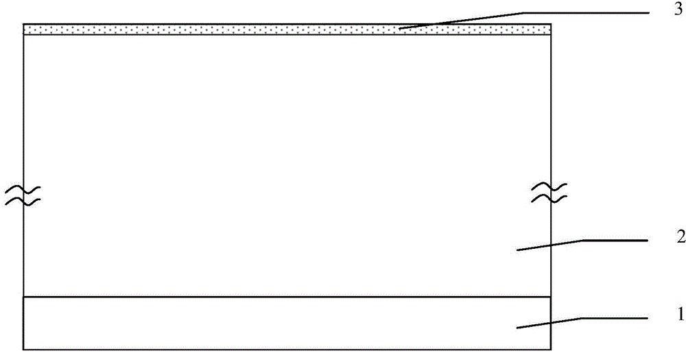
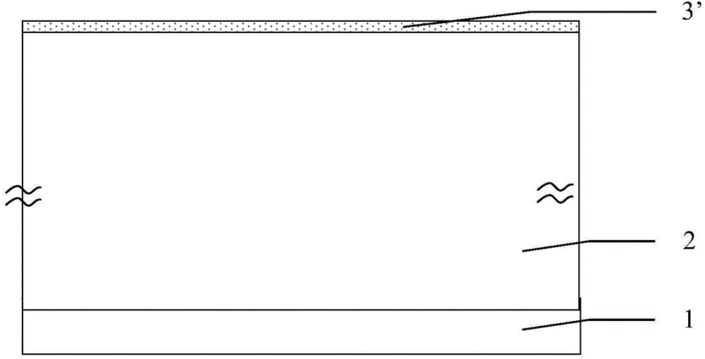
[0030] The invention improves on the basis of the traditional VDMOS manufacturing process, so that the VDMOS device has the anti-radiation performance. The specific principle is: the silicon dioxide gate oxide layer doped with aluminum impurities is used as the gate dielectric of the device, and the doped aluminum impurities are used as electron capture centers to reduce the accumulation of positive charges during irradiation and improve the ability to resist total dose radiation. At the same time, the dielectric constant of the gate medium is increased, the electric field in the gate medium is reduced when the device is irradiated, and the ability of the device to resist single-event gate breakdown is improved.

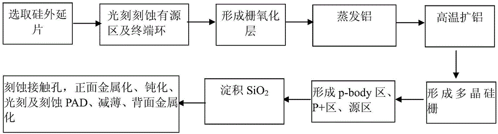
[0031] Concrete flow process of the present invention is as figure 1 As shown, an example is given to illustrate the specific implementation steps as follows:

[0032] (1) Choose a silicon epitaxial wafer with a crystal orientation of and a structure of N+N-, the r...


PUM


Abstract

The invention discloses a manufacture method of a VDMOS device with irradiation resistance. The manufacture method of the VDMOS device is characterized by forming a gate oxide layer, evaporating aluminum on the gate oxide layer, and then diffusing aluminum at high temperature to form a gate medium of an Si-O-Al structure. Positive charges accumulated in the gate medium can be reduced when the VDMOS device is irradiated; the resistance to total dose irradiation of the device is improved; meanwhile, compared with the conventional silicon dioxide gate medium, the gate medium of the Si-O-Al structure is higher in dielectric constant; the resistance to single event gate rupture of the device can be improved. The manufacture method can be used for effectively overcoming the contradiction of requirements on the thickness of the resistance to total dose irradiation and the single event gate rupture and optimizing the resistance to total dose irradiation and the single event gate rupture at the same time; the process is simple; the resistance to the irradiation of the VDMOS device is improved.

Description

technical field [0001] The invention relates to a method for manufacturing a VDMOS device with anti-radiation performance, belonging to the field of semiconductor device manufacturing. Background technique [0002] VDMOS is widely used in power circuits of space systems due to its advantages of fast switching speed, high input resistance, good frequency characteristics, high driving capability, and high transconductance linearity. There are a large number of charged particles and cosmic rays in the space, which will cause the parameters and performance of the device to degrade, and may fail in severe cases. In order to ensure the normal operation of the spacecraft, the anti-radiation reinforcement of VDMOS is of great significance. [0003] The total annual radiation dose received by earth satellites in near-earth orbit is 10Krad, and the total annual radiation dose received by earth satellites in far-earth orbit is 1000Krad. The performance degradation of VDMOS devices af...

Claims


Application Information

Patent Timeline
Patent Type & Authority Applications(China)
IPC IPC(8): H01L21/336H01L21/28
CPCH01L29/401H01L29/517H01L29/66712
Inventor 赵元富张文敏王传敏
Owner BEIJING MXTRONICS CORP
Why Eureka
Try Eureka