Semiconductor device having resin anti-bleed feature

a technology of semiconductor devices and resins, which is applied in the direction of semiconductor devices, semiconductor/solid-state device details, electrical equipment, etc., can solve the problems of increasing cost and/or valuable manufacturing time, reducing the reliability of the device, and reducing the use of resins. , to achieve the effect of preventing resin bleeding, increasing manufacturing costs, and increasing reliability

Active Publication Date: 2007-02-27
TEXAS INSTR INC
View PDF1 Cites 14 Cited by
  • Summary
  • Abstract
  • Description
  • Claims
  • Application Information

AI Technical Summary

Benefits of technology

[0008]In accordance with one aspect of the invention, the cap is bonded to one or more of the substrate and one or more electrical devices via an adhesive, wherein the adhesive is comprised of a plurality of components. For example, the adhesive generally resides on the surface of the substrate in the peripheral region, wherein the cap is further placed on the adhesive for bonding to the substrate. A first barrier is further formed over the surface of the substrate, wherein the first barrier generally resides between the adhesive and the exterior region of the surface of the substrate, wherein the first barrier generally prevents one or more of the plurality of components of the adhesive, such as a resin, from bleeding substantially onto the exterior region of the surface of the substrate.
[0009]A porosity of the first barrier, for example, is less than a porosity of one or more of the interior region and the exterior region of the surface of the substrate, wherein the porosity of the first barrier generally provides a capillary action to prevent the resin from bleeding onto the exterior region of the surface of the substrate. For example, the first barrier is comprised of a metal, wherein the porosity of the metal is substantially less than the porosity of the substrate, and wherein the resin flow is generally confined to a surface of the metal after reaching the first barrier. The first barrier, for example, is further formed on the surface of the substrate during a formation of other components associated with the device, such as a formation of bonding pads or electrical interconnects. Thus, the formation of the first barrier can be performed in a manner that does not require additional steps in processing the device, and can also increase reliability of the device without substantially increasing manufacturing costs. According to another aspect of the invention, the first barrier is formed substantially close to a side of the device, wherein minimal surface real estate is utilized to prevent bleeding of resin onto the exterior region of the substrate.

Problems solved by technology

Such a bleeding of the electrically-conductive bonding agent may provide further disadvantageous results in the finished device 10, such as an electrical shorting of various circuits, capacitance bleeding, etc.
However, as real estate on substrates becomes more and more valuable due to ever decreasing sizes of associated electronic devices, providing such a large area for resin bleed becomes less practical.
Additionally, conventional devices used to prevent the resin bleed typically require additional processing steps, therein adding cost and / or valuable manufacturing time.

Method used


Image

  • Semiconductor device having resin anti-bleed feature
  • Semiconductor device having resin anti-bleed feature
  • Semiconductor device having resin anti-bleed feature

Examples


Embodiment Construction

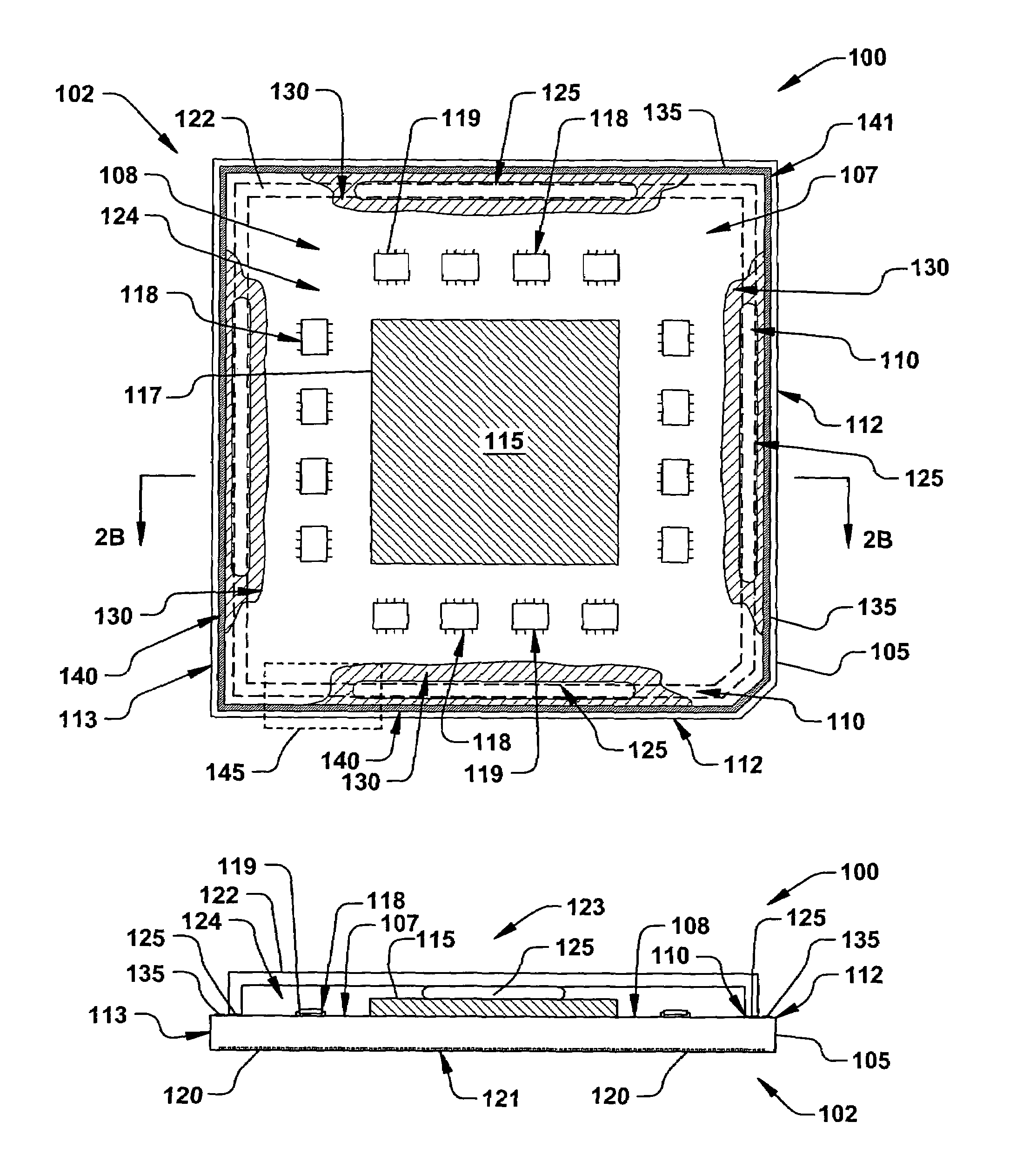
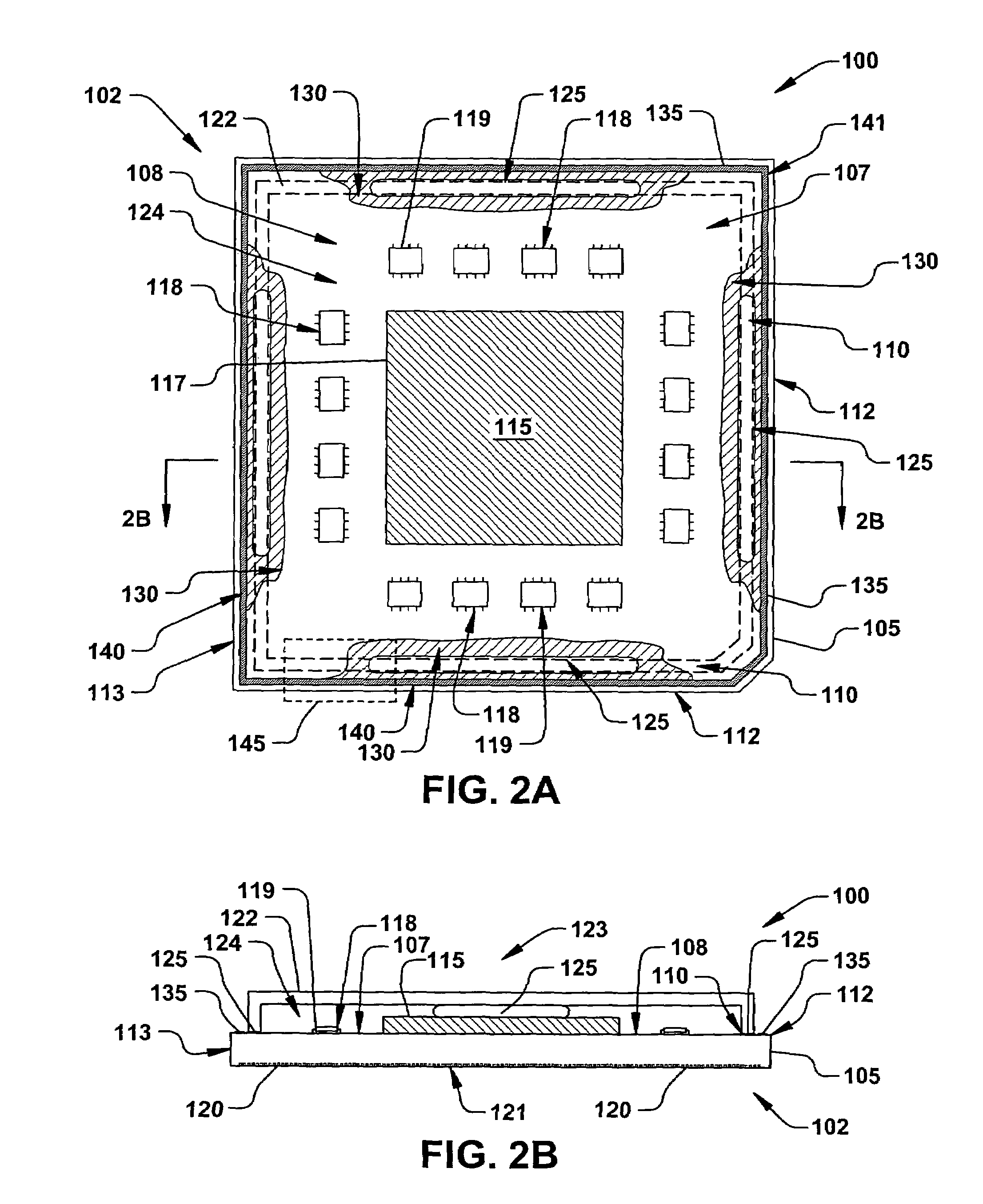
[0019]The present invention is directed towards a device for controlling a bleed of resin on a substrate. More particularly, the present invention provides a cost-effective solution for minimizing resin bleed into one or more regions of the substrate. Accordingly, the present invention will now be described with reference to the drawings, wherein like reference numerals are used to refer to like elements throughout. It should be understood that the description of these aspects are merely illustrative and that they should not be taken in a limiting sense. In the following description, for purposes of explanation, numerous specific details are set forth in order to provide a thorough understanding of the present invention. It will be evident to one skilled in the art, however, that the present invention may be practiced without these specific details.

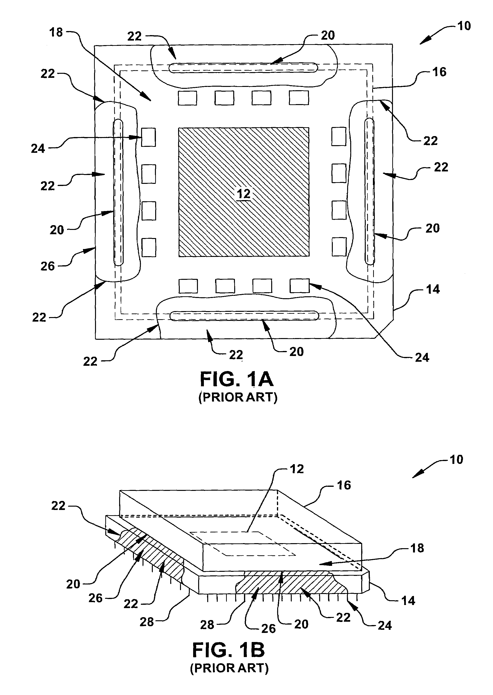
[0020]Referring now to the figures, FIG. 2A illustrates an exemplary electronic device 100, such as an integrated circuit package 102, i...


PUM


Abstract

A device and a method for controlling resin bleed, the device comprising a substrate having a surface, wherein an interior region, a peripheral region, and an exterior region of the surface are generally defined. An adhesive generally resides on the surface of the substrate in the peripheral region thereof, wherein the adhesive comprises a plurality of components, such as a metal and a resin. A first barrier is formed on the surface of the substrate generally between the adhesive and the exterior region, wherein the first barrier generally prevents one or more of the plurality of components of the adhesive from bleeding onto the exterior region of the surface of the substrate.

Description

FIELD OF THE INVENTION[0001]The present invention relates generally to semiconductor devices, and more particularly to a device for controlling a bleeding of resin on a substrate.BACKGROUND OF THE INVENTION[0002]In the semiconductor processing industry, various processes are performed on various substrates in order to form a multitude of various semiconductive components. For example, two or more differing components may be bonded to one another for purposes of electrical interconnection, heat dissipation, or to provide protection from environmental factors. In flip-chip semiconductor processing, for example, a conventional electronic device, such as the device 10 illustrated in FIG. 1A, comprises a flip-chip 12 that is bonded to a substrate 14, wherein the bond generally defines electrical connections (not shown) between the substrate and the flip-chip. Typically, the flip chip 12 is bonded to the substrate 14 via a plurality of solder balls, wherein the solder balls are melted in ...

Claims


Application Information

Patent Timeline
Patent Type & Authority Patents(United States)
IPC IPC(8): H01L23/48H01L23/29H01L23/34H01L23/52H01L29/40
CPCH01L23/10H01L23/564H01L2924/19105H01L2924/16152H01L2924/01079
Inventor FURTAW, ROBERT JOHNABBOTT, JOHN HENRYHOFFMAN, EMILY ELLEN
Owner TEXAS INSTR INC
Why Eureka
Try Eureka