Semiconductor memory

a technology of semiconductors and memory, applied in the field of semiconductor memory, can solve the problems of gate induced drain leakage (gidl) current, increase in standby current, serious problems, etc., and achieve the effect of reducing the gidl of transistors

Active Publication Date: 2007-02-27
SOCIONEXT INC
View PDF19 Cites 18 Cited by
  • Summary
  • Abstract
  • Description
  • Claims
  • Application Information

AI Technical Summary

Benefits of technology

[0014]It is an object of the present invention to reduce the GIDL of transistors that receive the boost voltage at their gates.
[0015]Another object of the present invention is to reduce the standby current of a semiconductor memory having dynamic memory cells without stopping the boost voltage generator thereof.
[0016]Still another object of the present invention is to reduce the standby current without an increase in access time.

Problems solved by technology

DRAMs and pseudo SRAMs need to perform periodic refresh operations on their memory cells even while the portable equipment is not in operation, and these refresh operations contribute to increases in standby currents.
Transistors supplied with the boost voltage at their gates are likely to have gate induced drain leakage (GIDL) currents.
In the semiconductor memories of this type, serious problems have thus occurred due to GIDL-based increases in the standby currents of transistors inside word drivers especially if the transistors receive the boost voltage at their gates.
This increases the voltage differences between the drains and the substrates or the voltage differences between the sources and the substrates, causing greater GIDL currents easily.
There has been no conventional technology for avoiding the occurrence of GIDL in the transistors receiving a boost voltage at their gates in a semiconductor memory that has dynamic memory cells and is supplied with the boost voltage for word lines.
This means deterioration in performance of the pseudo SRAM.
As a result, if the Reference 1 is applied to a pseudo SRAM in which a conflict can occur between access requests (read request and write request) and a refresh request, it takes a long time to make the first access after a refresh.
This leads to deterioration in performance of the pseudo SRAM since the access time in the product specification has to be set to the worst value.
For example, if the Reference 2 is applied to a DRAM which performs distributed refresh operations during the self-refresh mode, the standby current cannot be reduced satisfactorily due to a decrease in the stop period of the boost voltage generator and an increase in the frequency of stops and restarts thereof.

Method used


Image

  • Semiconductor memory
  • Semiconductor memory
  • Semiconductor memory

Examples


first embodiment

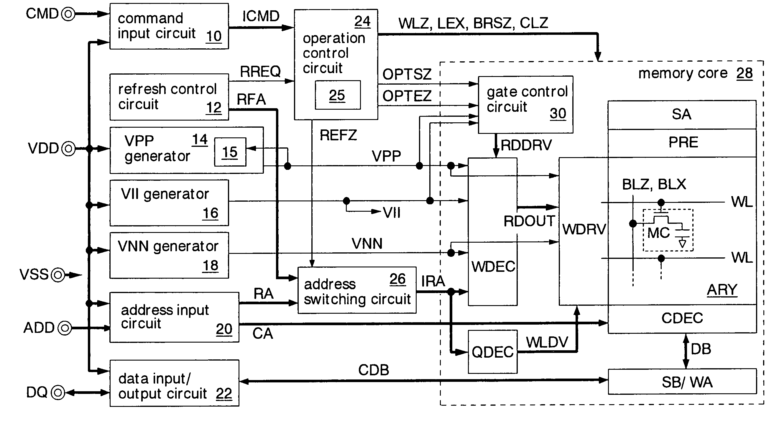
[0107]FIG. 4 shows an example where a refresh operation is performed during a standby period of the pseudo SRAM in the The standby periods STB in the diagram show periods in which no external command (read access request or write access command) is supplied, no refresh request occurs inside the pseudo SRAM, and the decoding units 32a of the word decoders WDEC shown in FIG. 3 are inactivated. The active period ACT is a period in which an external command is supplied or a refresh command occurs, and any of the decoding units 32a of the word decoders WDEC are activated.

[0108]In a standby period STB, the NOR circuits 30a shown in FIG. 3 receive the operation start signal OPTSZ and operation end signal OPTEZ of low level (VSS) (FIG. 4(a)), and output the operation signals OPTX of high level (VPP) (FIG. 4(b)). The operation signals OPTX of high level turn on the nMOS transistors 30b, so that the driving signals RDDRV are kept at the internal supply voltage VII (FIG. 4(c)). Since the outp...

second embodiment

[0138]The operation control circuit 24B outputs a self-refresh mode signal SREFX of low level in a self-refresh mode during which only a refresh operation is performed, responding to a refresh request signal RREQ generated by a refresh control circuit 12A and during which access requests are not accepted. The operation control circuit 24B outputs the self-refresh mode signal SREFX of high level in a normal operation mode during which the access requests (a read command, a write command, an auto-refresh command) are accepted. The other functions of the operation control circuit 24B are the same as those of the operation control circuit 24A of the second embodiment described above.

[0139]The gate control circuit 30B sets a row driving signal RDDRV (high-level voltage line) at a boost voltage VPP in the first period, i.e., active periods in a self-refresh mode and an entire period of the normal operation mode. The gate control circuit 30B sets the row driving signal RDDRV at an internal...

third embodiment

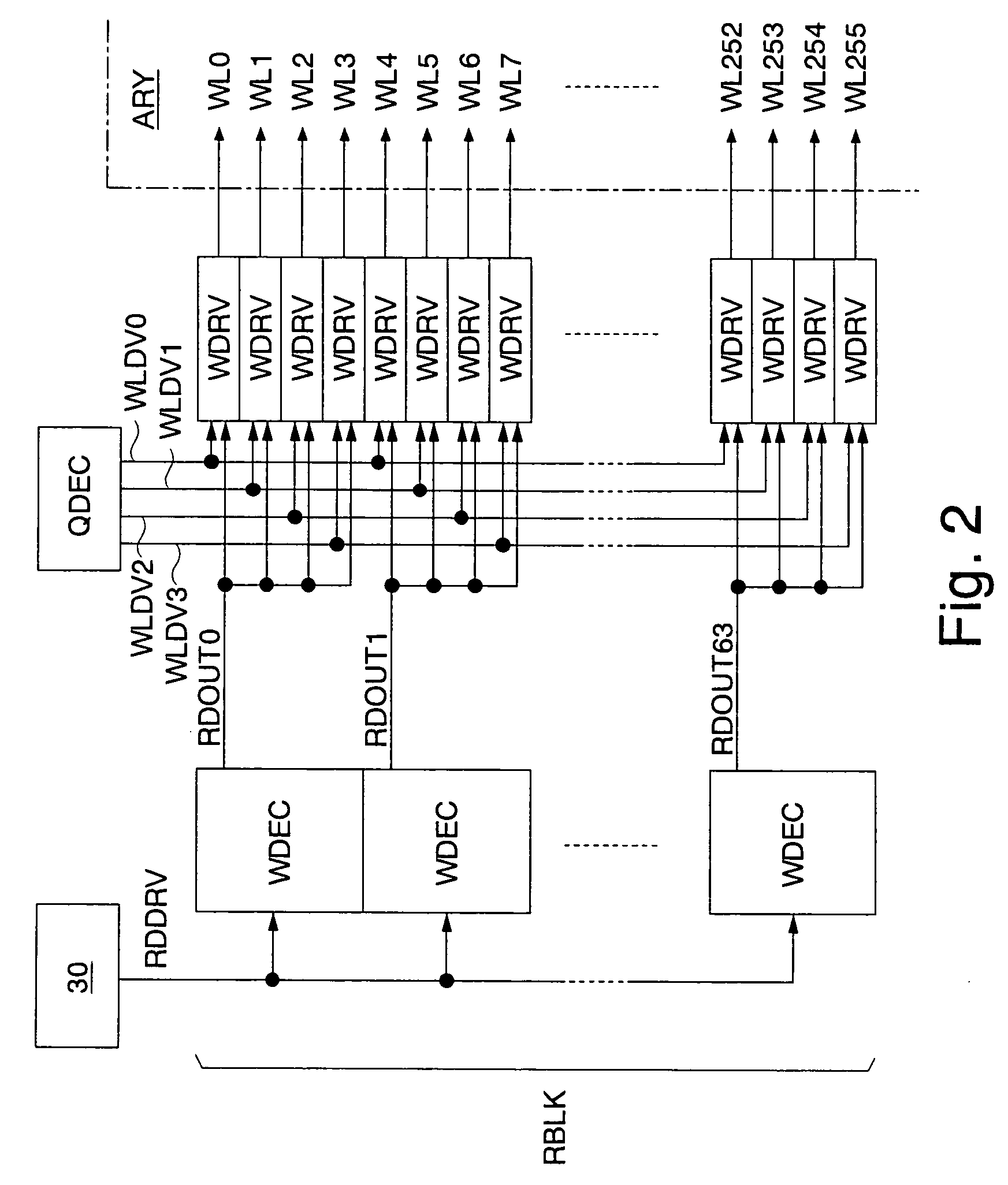
[0142]FIG. 10 shows an overview of operations of the DRAM in the Detailed description will be omitted of the same operations as in FIG. 4 and FIG. 5 described above. In this example, when receiving a self-refresh command during the normal operation mode, the DRAM shifts to the self-refresh mode, and when receiving a self-refresh releasing command during the self-refresh mode, it shifts to the normal operation mode.

[0143]In the normal operation mode, the self-refresh mode signal SREFX is kept at high level, and the operation signal OPTX is accordingly fixed to low level. Consequently, ON / OFF of the nMOS transistor 30b and the pMOS transistor 30c (switch circuit) shown in FIG. 9 is not switched over, and the high-level voltage line RDDRV is thus fixed to the boost voltage VPP. This eliminates power consumption for switching operations of the switch circuits 30b, 30c.

[0144]Specifically, the NOR circuit 30d does not drive the switch circuits 30b, 30c and thus consumes little power. In...


PUM


Abstract

A boost voltage generator generates a boost voltage as a high-level voltage of word lines. First word decoders output a low-level voltage or the high-level voltage according to a first address signal in an active period, and outputs the high-level voltage in a standby period. A switch circuit connects a high-level voltage line for supplying the high-level voltage to the first word decoders, with a boost voltage line in the active period, and connects the same with an internal voltage line in the standby period. The internal voltage line is supplied with a voltage lower than the boost voltage. Word drivers supply the boost voltage to the word lines when the gates of their transistors receive the low-level voltage from the first word decoders, and output the low-level voltage to the word lines when the gates thereof receive the high-level voltage from the first word decoders.

Description

CROSS REFERENCE TO RELATED APPLICATION[0001]This application is based upon and claims the benefit of priority from Japanese Patent Application No. 2003-370589, filed on Oct. 30, 2003, and No. 2004-191947, filed on Jun. 29, 2004, the entire contents of which are incorporated herein by reference.BACKGROUND OF THE INVENTION[0002]1. Field of the Invention[0003]The present invention relates to a semiconductor memory which has dynamic memory cells and word lines connected to the memory cells, and supplies a voltage higher than a power supply voltage to the word lines in accessing the memory cells.[0004]2. Description of the Related Art[0005]Recently, semiconductor memories having dynamic memory cells (DRAMs or pseudo SRAMs) have been used for work memories to be mounted on portable equipment such as a cellular phone. Since DRAM memory cells are smaller than SRAM memory cells, the use of DRAMs allows a reduction in product cost. In the meantime, semiconductor memories to be mounted on port...

Claims


Application Information

Patent Timeline
Patent Type & Authority Patents(United States)
IPC IPC(8): G11C8/00G11C8/08G11C11/407G11C11/403G11C11/406G11C11/408
CPCG11C8/08G11C11/4085G11C2211/4067G11C2207/2227
Inventor KOBAYASHI, HIROYUKIKANDA, TATSUYA
Owner SOCIONEXT INC
Why Eureka
Try Eureka