Semiconductor memory

a technology of semiconductors and memory, applied in the field of semiconductor memory, can solve the problems of gate induced drain leakage (gidl) current, increase in standby current, serious problems, etc., and achieve the effect of reducing gate induced drain leakage curren

Inactive Publication Date: 2005-05-19
FUJITSU LTD
View PDF4 Cites 20 Cited by
  • Summary
  • Abstract
  • Description
  • Claims
  • Application Information

AI Technical Summary

Benefits of technology

[0014] It is an object of the present invention to reduce the GIDL of transistors that receive the boost voltage at their gates.
[0015] Another object of the present invention is to reduce the standby current of a semiconductor memory having dynamic memory cells without stopping the boost voltage generator thereof.
[0016] Still another object of the present invention is to reduce the standby current without an increase in access time.

Problems solved by technology

DRAMs and pseudo SRAMs need to perform periodic refresh operations on their memory cells even while the portable equipment is not in operation, and these refresh operations contribute to increases in standby currents.
Transistors supplied with the boost voltage at their gates are likely to have gate induced drain leakage (GIDL) currents.
In the semiconductor memories of this type, serious problems have thus occurred due to GIDL-based increases in the standby currents of transistors inside word drivers especially if the transistors receive the boost voltage at their gates.
This increases the voltage differences between the drains and the substrates or the voltage differences between the sources and the substrates, causing greater GIDL currents easily.
There has been no conventional technology for avoiding the occurrence of GIDL in the transistors receiving a boost voltage at their gates in a semiconductor memory that has dynamic memory cells and is supplied with the boost voltage for word lines.
This means deterioration in performance of the pseudo SRAM.
As a result, if the Reference 1 is applied to a pseudo SRAM in which a conflict can occur between access requests (read request and write request) and a refresh request, it takes a long time to make the first access after a refresh.
This leads to deterioration in performance of the pseudo SRAM since the access time in the product specification has to be set to the worst value.
For example, if the Reference 2 is applied to a DRAM which performs distributed refresh operations during the self-refresh mode, the standby current cannot be reduced satisfactorily due to a decrease in the stop period of the boost voltage generator and an increase in the frequency of stops and restarts thereof.

Method used


Image

  • Semiconductor memory
  • Semiconductor memory
  • Semiconductor memory

Examples


first embodiment

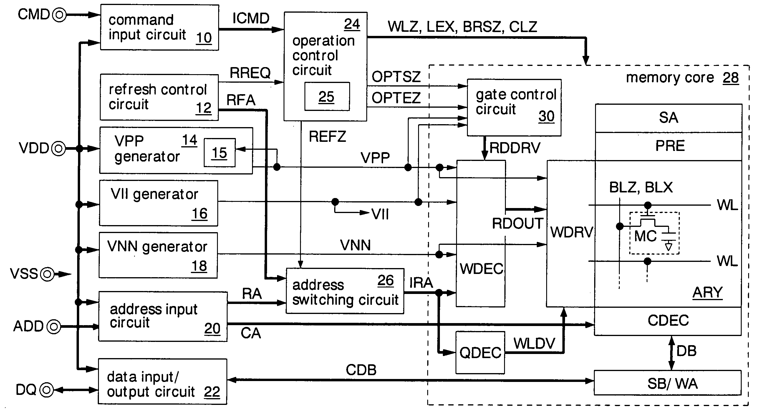
[0046]FIG. 1 shows the semiconductor memory of the present invention. This semiconductor memory is formed as a pseudo SRAM chip on a silicon substrate by using CMOS processes. The pseudo SRAM has a DRAM memory core and an SRAM interface. The pseudo SRAM performs periodic refresh operations inside the chip without receiving refresh commands from exterior, thereby retaining data written in its memory cells. The pseudo SRAM is used, for example, as a work memory to be mounted on a cellular phone. A read operation and a write operation are performed in accordance with command signals CMD (a read command and a write command) supplied through an external terminal.

[0047] The pseudo SRAM has a command input circuit 10, a refresh control circuit 12, a VPP generator 14, a VII generator 16, a VNN generator 18, an address input circuit 20, a data input / output circuit 22, an operation control circuit 24, an address switching circuit 26, and a memory core 28. Incidentally, FIG. 1 only shows essen...

second embodiment

[0114] The foregoing second embodiment has dealt with the case where the present invention is applied to a DRAM having an auto refresh function. However, the present invention is not limited to such an embodiment. For example, the present invention may be applied to a DRAM which receives a refresh command along with a refresh address.


PUM


Abstract

A boost voltage generator generates a boost voltage as a high-level voltage of word lines. First word decoders output a low-level voltage or the high-level voltage according to a first address signal in an active period, and outputs the high-level voltage in a standby period. A switch circuit connects a high-level voltage line for supplying the high-level voltage to the first word decoders, with a boost voltage line in the active period, and connects the same with an internal voltage line in the standby period. The internal voltage line is supplied with a voltage lower than the boost voltage. Word drivers supply the boost voltage to the word lines when the gates of their transistors receive the low-level voltage from the first word decoders, and output the low-level voltage to the word lines when the gates thereof receive the high-level voltage from the first word decoders.

Description

CROSS REFERENCE TO RELATED APPLICATION [0001] This application is based upon and claims the benefit of priority from Japanese Patent Application No. 2003-370589, filed on Oct. 30, 2003, the entire contents of which are incorporated herein by reference.BACKGROUND OF THE INVENTION [0002] 1. Field of the Invention [0003] The present invention relates to a semiconductor memory which has dynamic memory cells and word lines connected to the memory cells, and supplies a voltage higher than a power supply voltage to the word lines in accessing the memory cells. [0004] 2. Description of the Related Art [0005] Recently, semiconductor memories having dynamic memory cells (DRAMs or pseudo SRAMs) have been used for work memories to be mounted on portable equipment such as a cellular phone. Since DRAM memory cells are smaller than SRAM memory cells, the use of DRAMs allows a reduction in product cost. In the meantime, semiconductor memories to be mounted on portable equipment require low power co...

Claims


Application Information

Patent Timeline
Patent Type & Authority Applications(United States)
IPC IPC(8): G11C8/08G11C11/408
CPCG11C2207/2227G11C8/08
Inventor KANDA, TATSUYA
Owner FUJITSU LTD
Why Eureka
Try Eureka