Method of manufacturing a semiconductor package

a manufacturing method and semiconductor technology, applied in the direction of semiconductor/solid-state device details, conductive pattern formation, printed element electric connection formation, etc., can solve the problem that the packaging is typically not compatible with existing integrated circuit packages, and achieve the effect of improving plating uniformity

Inactive Publication Date: 2007-03-06
AMKOR TECH SINGAPORE HLDG PTE LTD
View PDF125 Cites 386 Cited by
  • Summary
  • Abstract
  • Description
  • Claims
  • Application Information

AI Technical Summary

Problems solved by technology

However, such packaging is typically not compatible with existing integrated circuit packages, so that two or more integrated circuits that are “stacked” must all be designed for stacking.

Method used


Image

  • Method of manufacturing a semiconductor package
  • Method of manufacturing a semiconductor package
  • Method of manufacturing a semiconductor package

Examples


Embodiment Construction

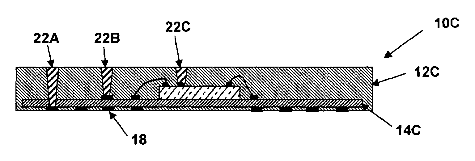
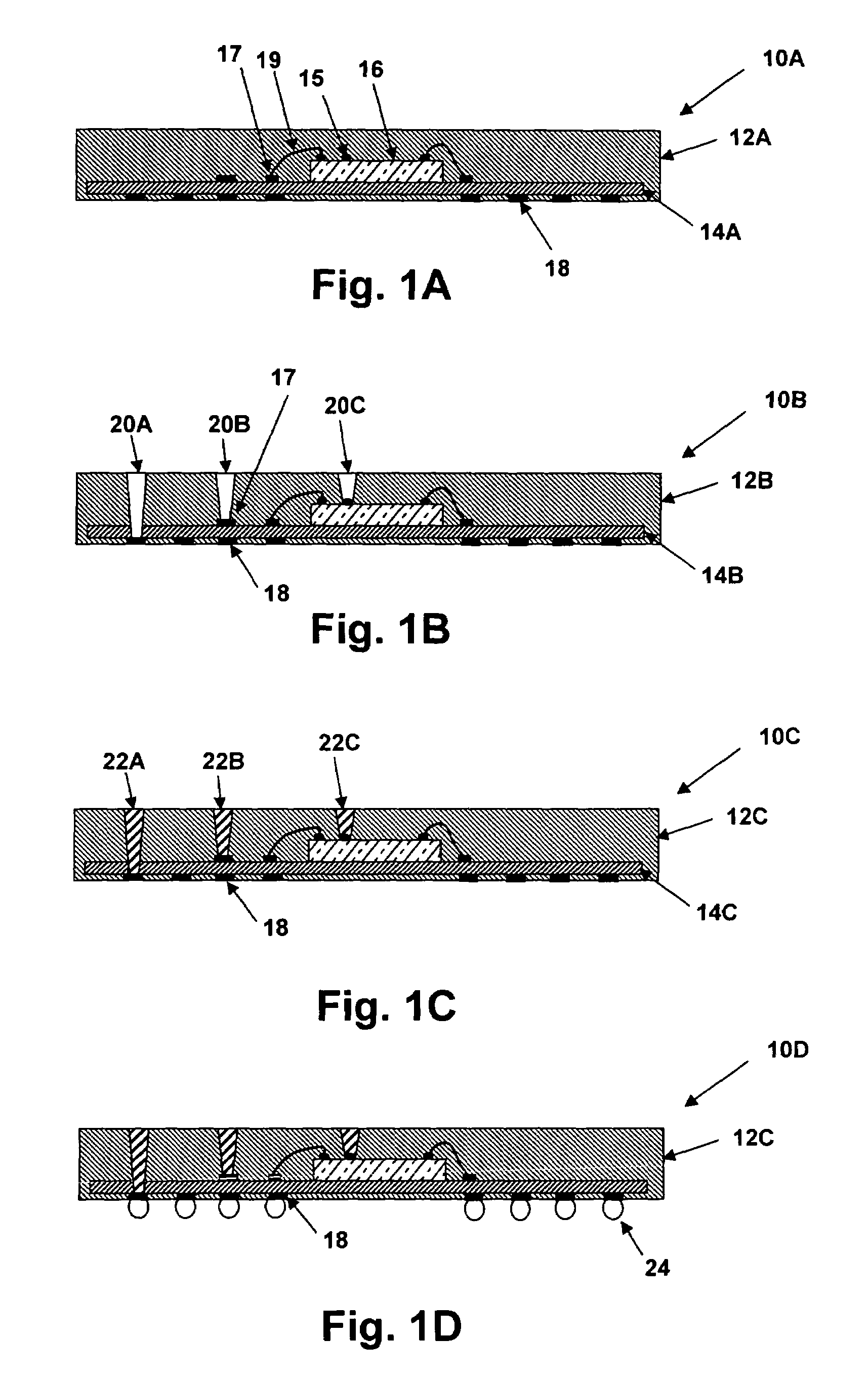
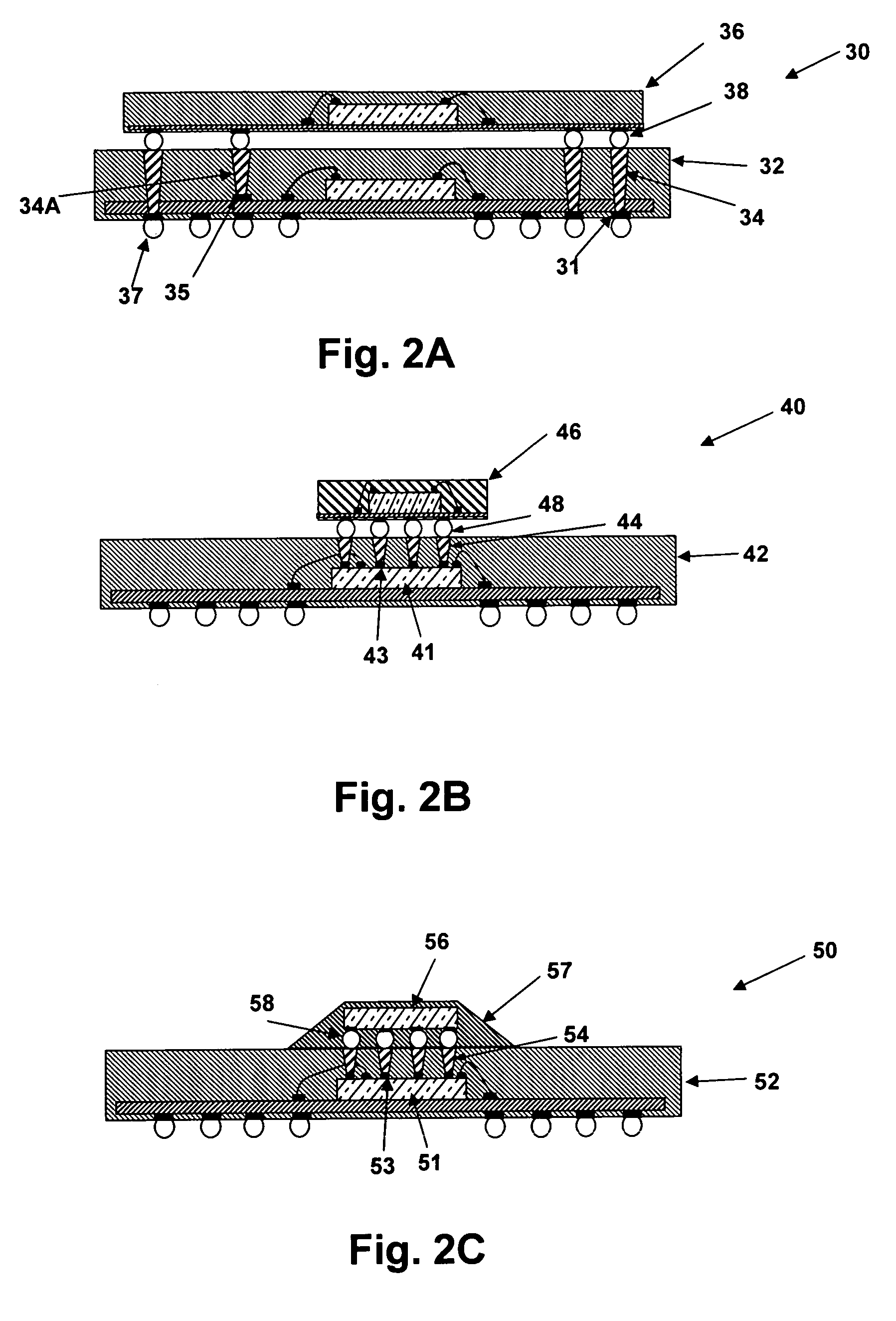
[0018]The present invention concerns a semiconductor package and a method for manufacturing a semiconductor package that provide for top mounting of another semiconductor package in a “piggyback” configuration. While the exemplary embodiments depict ball grid array packages mounted atop a plurality of lands on the top side of a modified semiconductor package, it should be understood by those skilled in the art, that the techniques of the present invention can be extended to other types of semiconductor interconnects.

[0019]Referring now to FIG. 1A, a semiconductor package 10A for forming a semiconductor package and corresponding to a first illustrated step of manufacture is depicted. Semiconductor package 10A is in the form of a ball grid array (BGA) or land grid array (LGA) package as is commonly known in the art, except that particular circuit features are positioned for providing vias to the top side of semiconductor package 10A in subsequent manufacturing steps, so that another s...


PUM

PropertyMeasurementUnit
conductiveaaaaaaaaaa
electricalaaaaaaaaaa
CONDUCTIVEaaaaaaaaaa

Abstract

A semiconductor package including top-surface terminals for mounting another semiconductor package provides a three-dimensional circuit configuration that can provide removable connection of existing grid-array packages having a standard design. A semiconductor die is mounted on an electrically connected to a circuit substrate having terminals disposed on a bottom side for connection to an external system. The die and substrate are encapsulated and vias are laser-ablated or otherwise formed through the encapsulation to terminals on the top surface of the substrate that provide a grid array mounting lands to which another grid array semiconductor package may be mounted. The bottom side of the vias may terminate and electrically connect to terminals on the substrate, terminals on the bottom of the semiconductor package (through terminals) or terminals on the top of the semiconductor die. The vias may be plated, paste-filled, filled with a low melting point alloy and may have a conical profile for improved plating performance.

Description

CROSS-REFERENCE TO RELATED APPLICATIONS[0001]The present application is a continuation-in-part of U.S. patent application “INTEGRATED CIRCUIT SUBSTRATE HAVING LASER-EMBEDDED CONDUCTIVE PATTERNS AND METHOD THEREFOR”, Ser. No. 10 / 138,225 filed on May 1st, 2002, now U.S. Pat. No. 6,930,256, issued Aug. 16, 2005, by at least one common inventor and assigned to the same assignee. The specification of the above-referenced Patent Application is herein incorporated by reference.FIELD OF THE INVENTION[0002]The present invention relates generally to semiconductor packaging, and more specifically, to a semiconductor package having top-surface grid array terminals for mounting another semiconductor package.BACKGROUND OF THE INVENTION[0003]Semiconductor packages that provide mechanical mounting and electrical interconnection of a semiconductor die are commonly provided in ball grid array and land grid array configurations. A semiconductor die is electrically connected to a substrate with a grid ...

Claims


Application Information

Patent Timeline
Patent Type & Authority Patents(United States)
IPC IPC(8): H05K3/30H01L21/48H05K1/05H05K3/00H05K3/10H05K3/12H05K3/42H05K7/10
CPCH01L21/4857H05K3/107H05K3/1258H05K7/1061H01L24/73Y10T29/49146H01L2224/16H01L2224/48091H01L2924/01029H01L2924/01078H01L2924/01079H01L2924/01082H01L2924/14H01L2924/15311H05K1/056H05K3/0032H05K3/0035H05K3/423H05K2201/09036H05K2201/09554H05K2203/0723Y10T29/49165Y10T29/4913Y10T29/49126Y10T29/49155Y10T29/49167H01L2924/1815H01L2224/48227H01L2224/73265H01L2224/32225H01L2924/014H01L2924/01005H01L2924/01006H01L2924/01033H01L2924/01047H01L2924/00014H01L2924/00012H01L2924/00H01L2924/15747
Inventor HINER, DAVID JONHUEMOELLER, RONALD PATRICKRUSLI, SUKIANTO
Owner AMKOR TECH SINGAPORE HLDG PTE LTD
Why Eureka
Try Eureka