

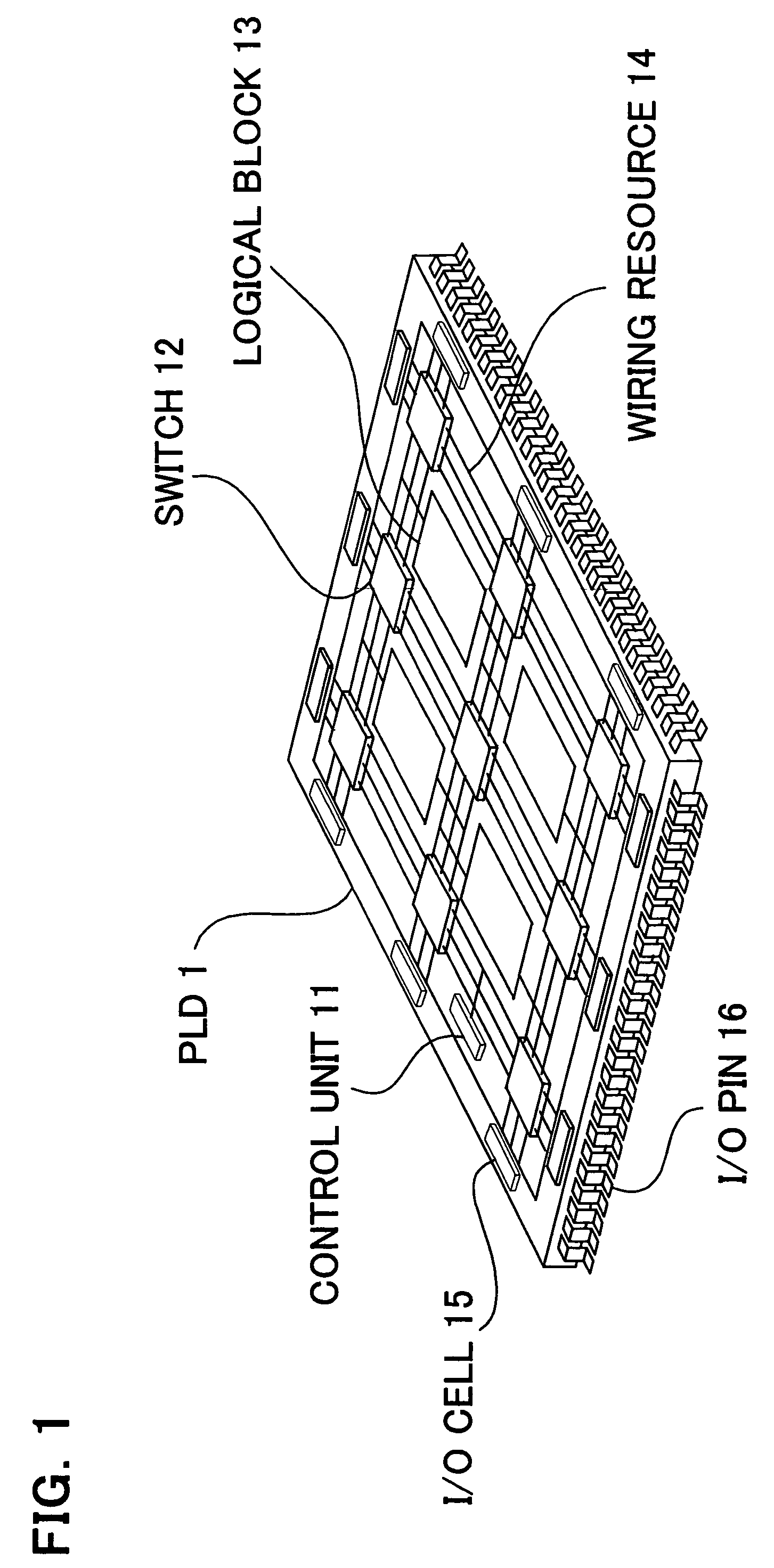
Programmable logic device
a logic device and programmable logic technology, applied in the direction of instruments, computation using denominational number representation, pulse technique, etc., can solve the problems of not being able to deal with defects, not being able to deal with such defects, etc., and achieve the effect of improving the product yield by avoiding defects
- Summary
- Abstract
- Description
- Claims
- Application Information
AI Technical Summary
Benefits of technology
Problems solved by technology
Method used
Image

Examples
first embodiment
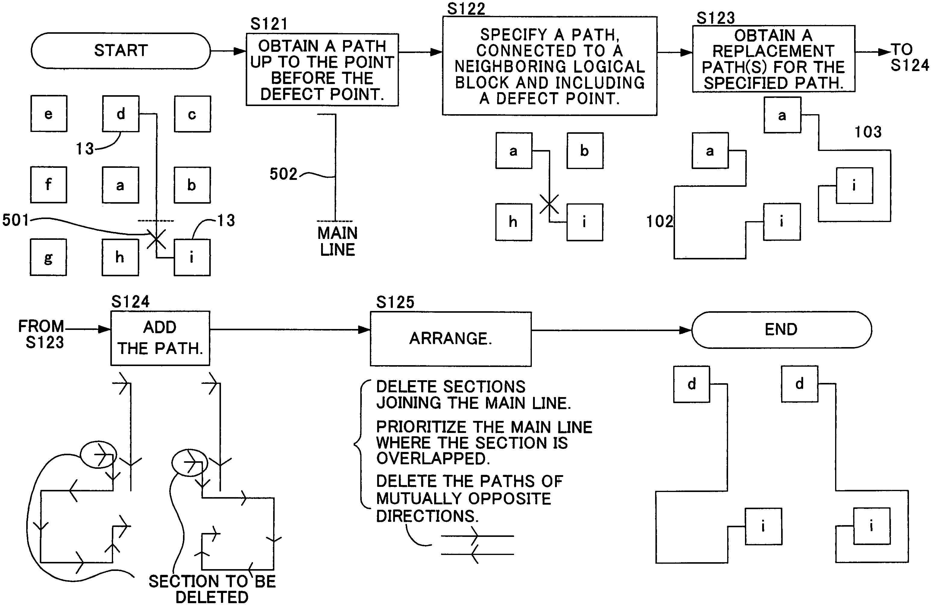
[0085] a process for diverting from a defect point is performed when initiating a PLD. The PLD then refers to the defect point information and circuit information, and according to the circuit information, when a path for realizing a predetermined logic circuit to be formed from now has a fault resource, the PLD refers to the replacement rule table, induces a replacement path(s), and controls switch 12 so as to divert the fault resource.
[0086]FIGS. 11A, 11B are functional block diagrams each illustrating a control unit 11 of PLD 1 according to the first embodiment of the present invention. FIG. 11A represents a state of control unit 11 in a write phase, up to when circuit information is stored into the PLD, while FIG. 11B represents a state of control unit 11 in an initiation phase after the PLD is initiated.
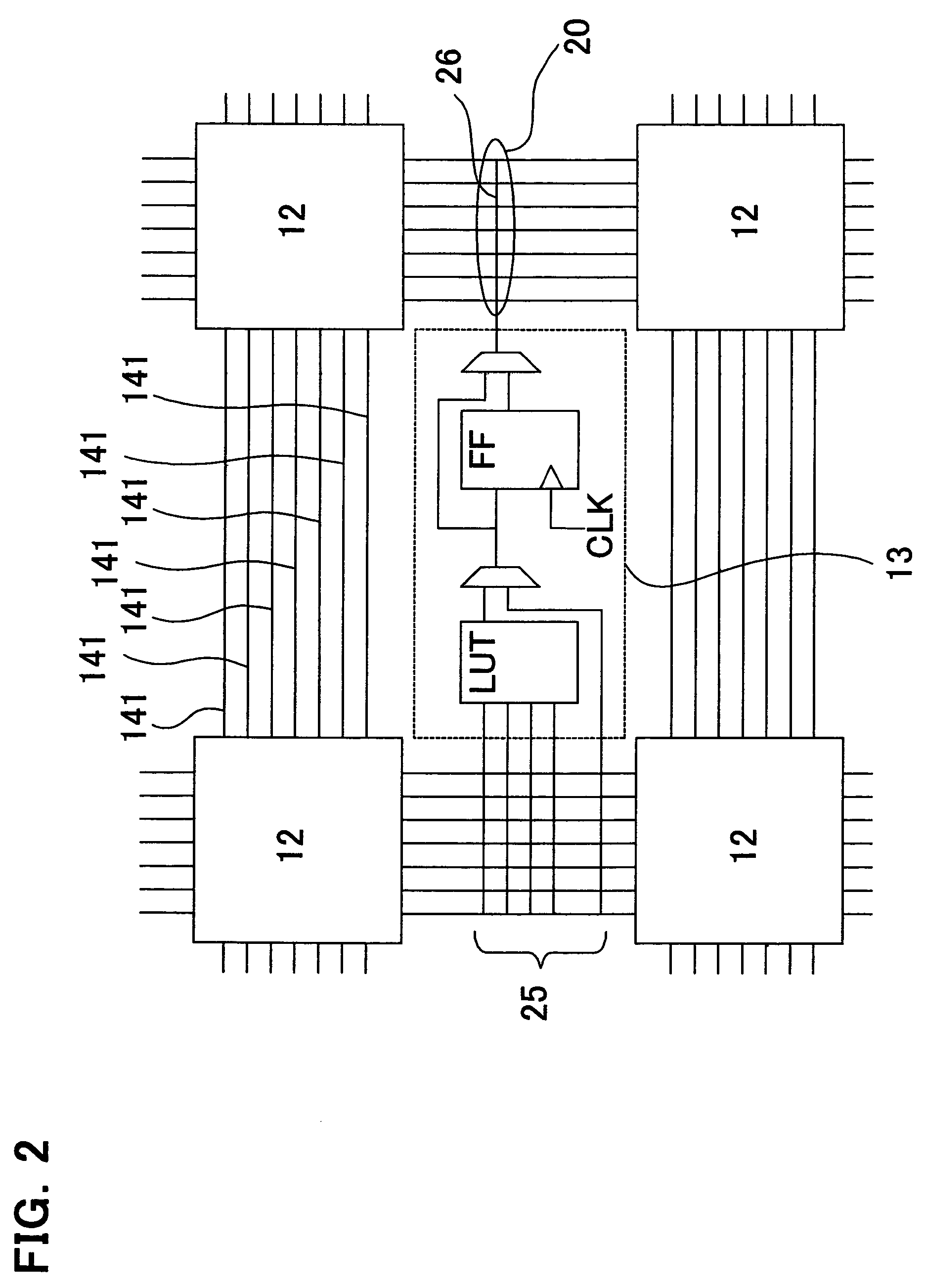
[0087]A control unit 11 shown in FIGS. 11A, 11B includes a controller 60 and a storage 74. Controller 60 further includes a replacement control section 72 and a wiring resource ...
second embodiment
[0098]FIGS. 13A, 13B are functional block diagrams each illustrating control unit 11 of PLD 1 according to the present invention. FIG. 13A represents the state of control unit 11 in the write phase up to when circuit information is stored into the PLD, while FIG. 13B represents the state of control unit 11 in the initiation phase after the PLD is initiated.
[0099]A control unit 11 shown in FIGS. 13A, 13B includes a controller 60 and a storage 74. Controller 60 further includes a write control section 71, a replacement control section 72 and a wiring resource section 73. Each functional section in controller 60 is realized by programs executed in a non-illustrated CPU provided in controller 60, or can be realized by hardware.
[0100]As described earlier in regard to the premise, storage 74 includes defect point information 51 (refer to FIG. 8) and a replacement rule table 52 (refer to FIG. 9B) in advance. In FIG. 13A, when storing the circuit information, write control section 71 perfor...
third embodiment
[0110]FIGS. 15A, 15B show functional block diagrams each illustrating control unit 11 of PLD 1 according to the present invention. FIG. 15A represents a state of control unit 11 in a write phase up to when circuit information is stored into the PLD, while FIG. 15B represents a state of control unit 11 in an initiation phase after the PLD is initiated.
[0111]Control unit 11 shown in FIGS. 15A, 15B includes a controller 60 and a storage 74. Controller 60 further includes write control section 71 and wiring resource section 73. Each functional section in controller 60 is realized by programs executed in a non-illustrated CPU provided in controller 60, or can be realized by hardware.
[0112]As described earlier in regard to the premise, storage 74 includes defect point information 51 (refer to FIG. 8) and a replacement rule table 52 (refer to FIG. 9B) in advance. The operation in a write phase shown in FIG. 15A is identical to that in the second embodiment, and therefore the explanation is...
PUM
 Abstract
Description
Claims
Application Information