Capacity dividable memory IC

a memory and capacity technology, applied in the field of memory integrated circuits, can solve the problems of one half of memory being left unused and wasted, and each set of masks can only yield a single capacity memory, so as to prevent material damage and yield different capacity memories

Inactive Publication Date: 2007-03-13
LYONTEK
View PDF21 Cites 3 Cited by
  • Summary
  • Abstract
  • Description
  • Claims
  • Application Information

AI Technical Summary

Benefits of technology

[0005]An object of the present invention is to provide a memory layout which can yield different capacity memories. Another object of the invention is to provide a memory layout which can furnish memory IC with half of the memory capacity through physically cutting half of the original memory IC. Still another object of the invention is to use the same of masks to divide and subdivide the memory capacity of an IC. A further object of the present invention is to prevent material damage when a chip is sawed to yield two half capacity memory areas.

Problems solved by technology

If a half capacity memory is needed, one half of memory is left unused and wasted, because there is no way to cut the memory into half capacity memory.
In other words, each set of masks can only yield a single capacity memory.

Method used


Image

  • Capacity dividable memory IC
  • Capacity dividable memory IC
  • Capacity dividable memory IC

Examples


Embodiment Construction

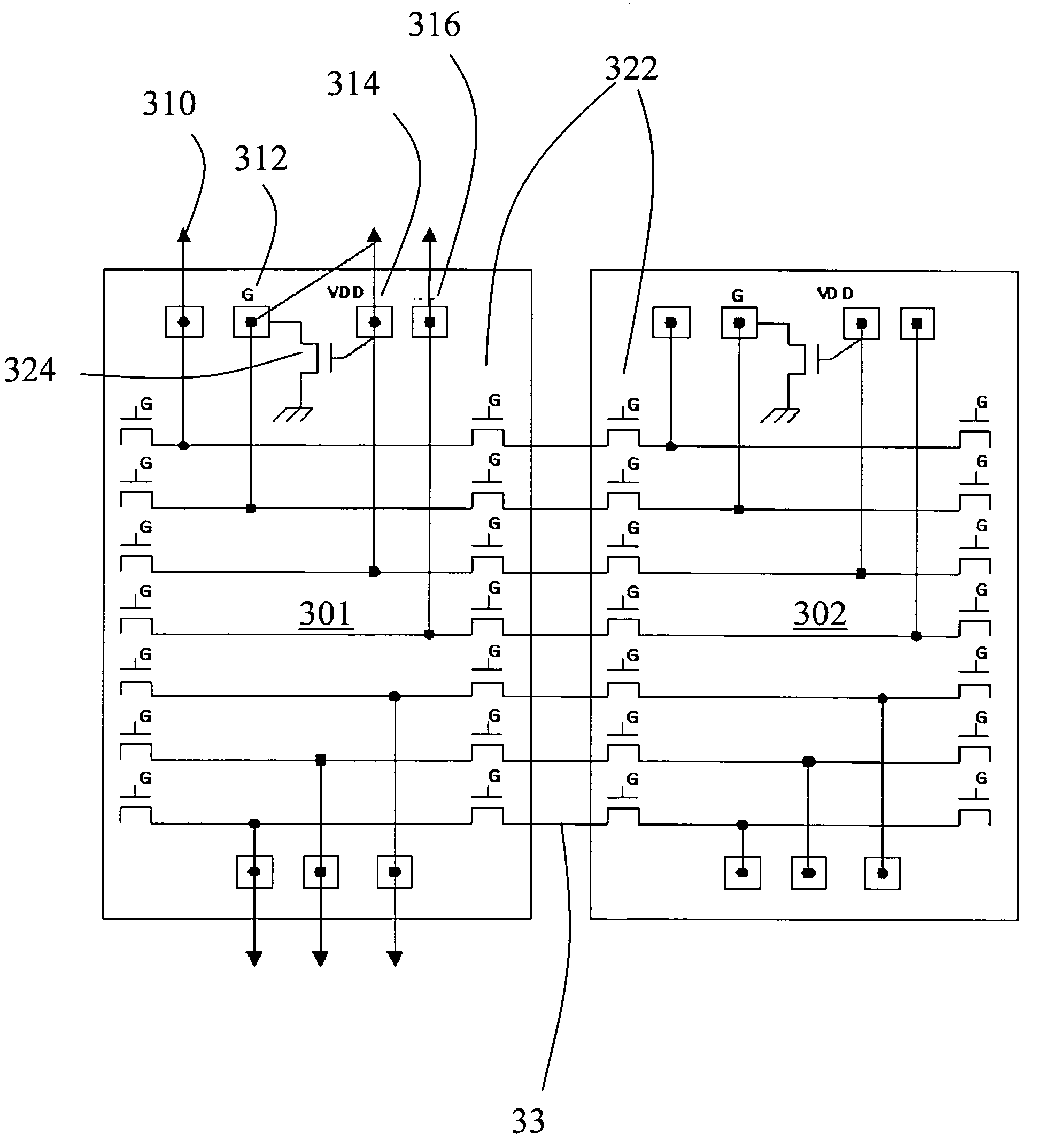
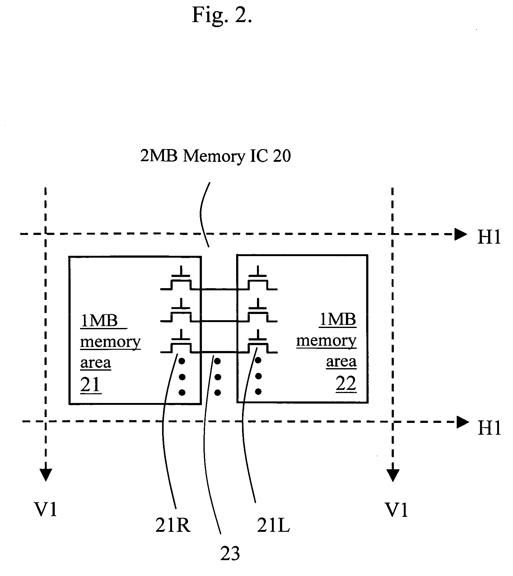
[0012]FIG. 2 shows the basic concept of the present invention. Two 1 MB memory areas 21 and 22 on a common substrate are joined together to form a 2 MB memory IC 20. The adjoining sides of the two areas are lined with pass transistors: pass transistors 21R at the left memory area 21, and pass transistor 21L at the right memory area 22. These pass transistors are MOSFETs, connected with interconnections 23. The gates of the pass transistors along the same column are in common. The pass transistors are turned on and off by applying a control signal at the common gates. Each pass transistor is connected to a functional bonding pad such as positive power supply VDD, Ground GD, signal pads, etc. of the individual memory area as shown in FIG. 5. Each adjoining pair of the pass transistors corresponds to a dedicated functional pad. When the adjoining pass transistors are turned on or activated, the two 1 MB memory areas 21 and 22 are connected in parallel, and the memory capacity is double...


PUM


Abstract

Two memory areas on a wafer are coupled through pass transistors to double the memory capacity of each area and can be sawed to yield two memory chips each with single memory area. A pair of pass transistors are used to couple each dedicated functional pad in both memory areas, when the pass transistors are turned on. The connection between the pass transistor pair can be sawed through to yield single capacity memory dice. The memory capacity can be further increased by coupling more memory areas together with pass transistors.

Description

BACKGROUND OF THE INVENTION[0001]1. Field of the Invention[0002]This invention relates to memory integrated circuit (IC), in particular to memory IC which can be divided to yield different capacity memories.[0003]2. Brief Description of Related Art[0004]FIG. 1 shows a prior art memory IC 10 as an example. Each IC chip can yield a single capacity memory. If a half capacity memory is needed, one half of memory is left unused and wasted, because there is no way to cut the memory into half capacity memory. If it is desired to reduce cost and to double the profit, a different product must be designed using different sets of production masks. When a customer requires different capacity memory ICs, a different set of dedicated masks must be provided for each memory capacity. In other words, each set of masks can only yield a single capacity memory.SUMMARY OF THE INVENTION[0005]An object of the present invention is to provide a memory layout which can yield different capacity memories. Anot...

Claims


Application Information

Patent Timeline
Patent Type & Authority Patents(United States)
IPC IPC(8): G11C5/06G11C11/06G11C8/00
CPCG11C5/06
Inventor HUNG, CHI-CHENGCHANG, LING-YUEHCHUNG, PWU-YUEH
Owner LYONTEK
Why Eureka
Try Eureka