
Flexible capacity memory IC

a memory and flexible technology, applied in the field of expandable ic memory, can solve the problem of inability to obtain double capacity, and achieve the effect of expanding memory capacity

Inactive Publication Date: 2006-12-21
LYONTEK
View PDF8 Cites 4 Cited by
  • Summary
  • Abstract
  • Description
  • Claims
  • Application Information

AI Technical Summary

Benefits of technology

"The present invention provides a method and product that allows for the expansion of memory capacity without requiring major changes in IC design and manufacturing process. This is achieved by adding a \"selector pad\" on each basic memory area unit, which controls a single-pole, double-throw switch. This allows for the separation of memory areas on a wafer to yield appropriate memory capacity dice. The invention provides a single design process with or without using additional two mask layers that can meet the choices from two memory capacity products. This reduces production cost and provides flexibility in IC layout for different memory capacity."

Problems solved by technology

In traditional practice, the double capacity cannot be obtained from combining two of the single capacity memory areas at wafer stage.

Method used


Image

  • Flexible capacity memory IC
  • Flexible capacity memory IC
  • Flexible capacity memory IC

Examples


Embodiment Construction

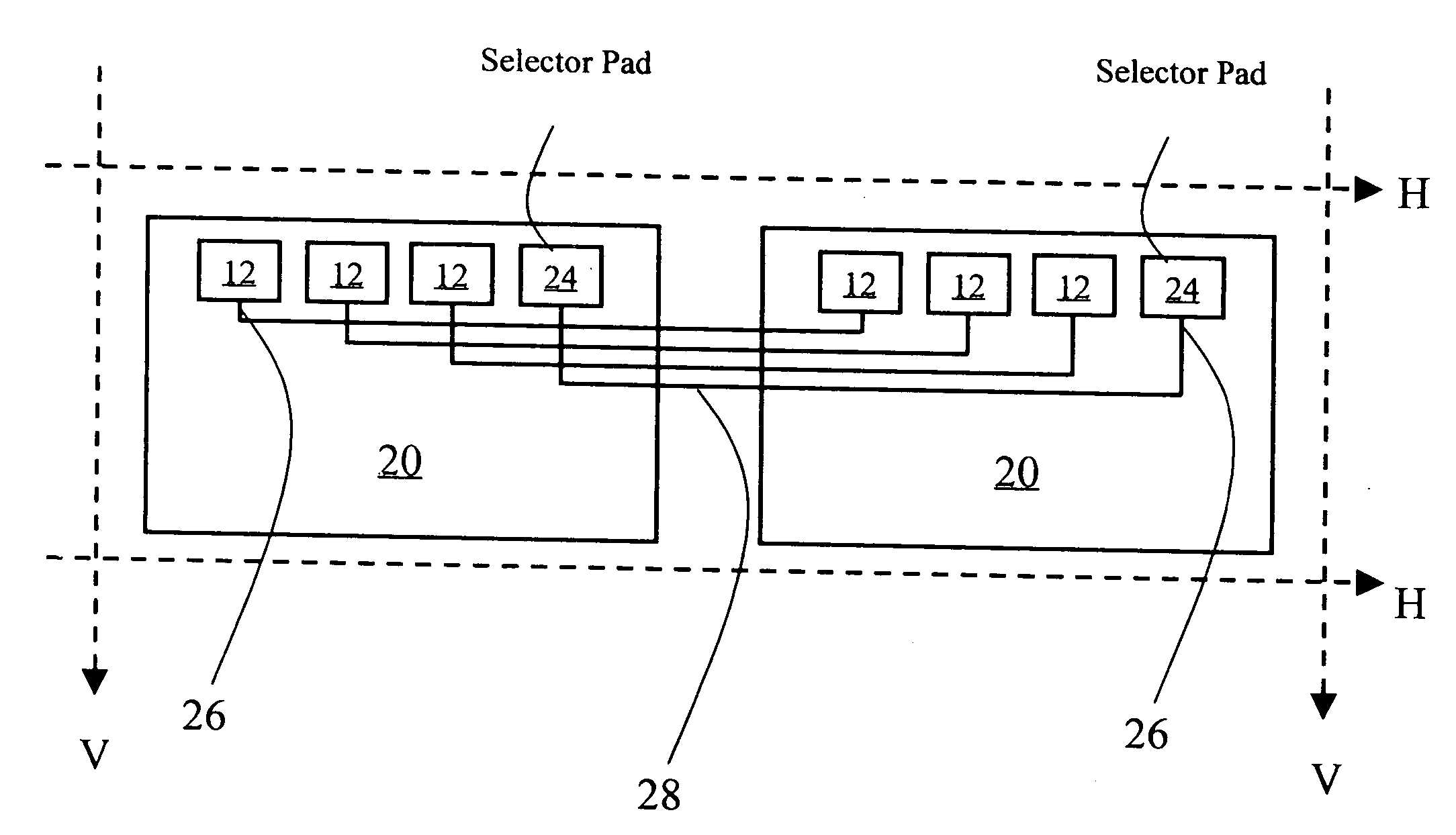
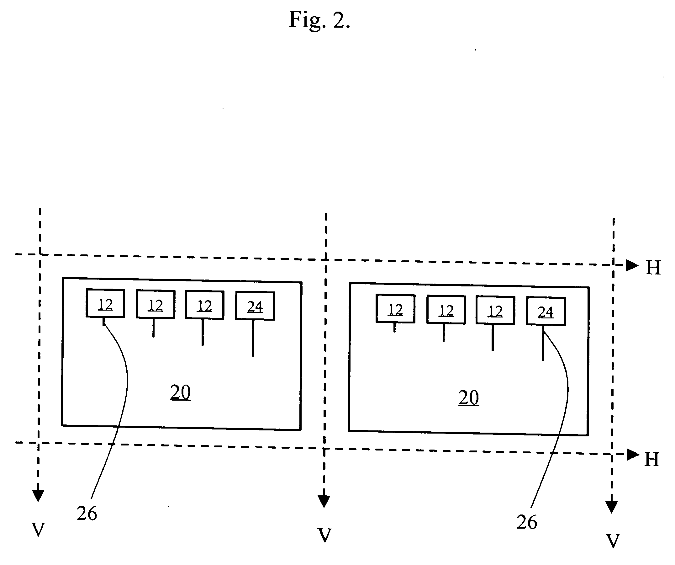
[0011]FIG. 2 shows the basic layout of the present invention. A number of substantially the same memory IC areas 20 are laid out on a common wafer. On each memory area 20, there are numerous signal pads 12. A selector pad 24 is laid out on each memory area 20. The selector pad 24 controls a single-pole, double-throw (STDP) switch or 1-bit decoder (not shown), which enables or disables the area on which the selector pad is placed. In manufacturing single capacity memory, dice are fabricated by sawing through the vertical line V2 and the horizontal line H2 in FIG. 2 to yield single capacity memory chips 20. The selector pad 24 presets the STDP or the 1-bit decoder to a fixed logic state (for example, logic “0” state). In order to manufacture double capacity memory ICs product, two neighboring chip areas 20 can be integrated as a unit in wafer stage to provide double memory capacity. As shown in FIG. 3, double capacity memory is fabricated through combining two single capacity memory a...


PUM


Abstract

More than one memory areas are connected in parallel to increase the memory capacity when activated. The different memory area in a single unit die is activated by a selector pad which controls a single-pole, double throw switch to enable or disable the different memory areas. The corresponding pads of like memory areas are interconnected.

Description

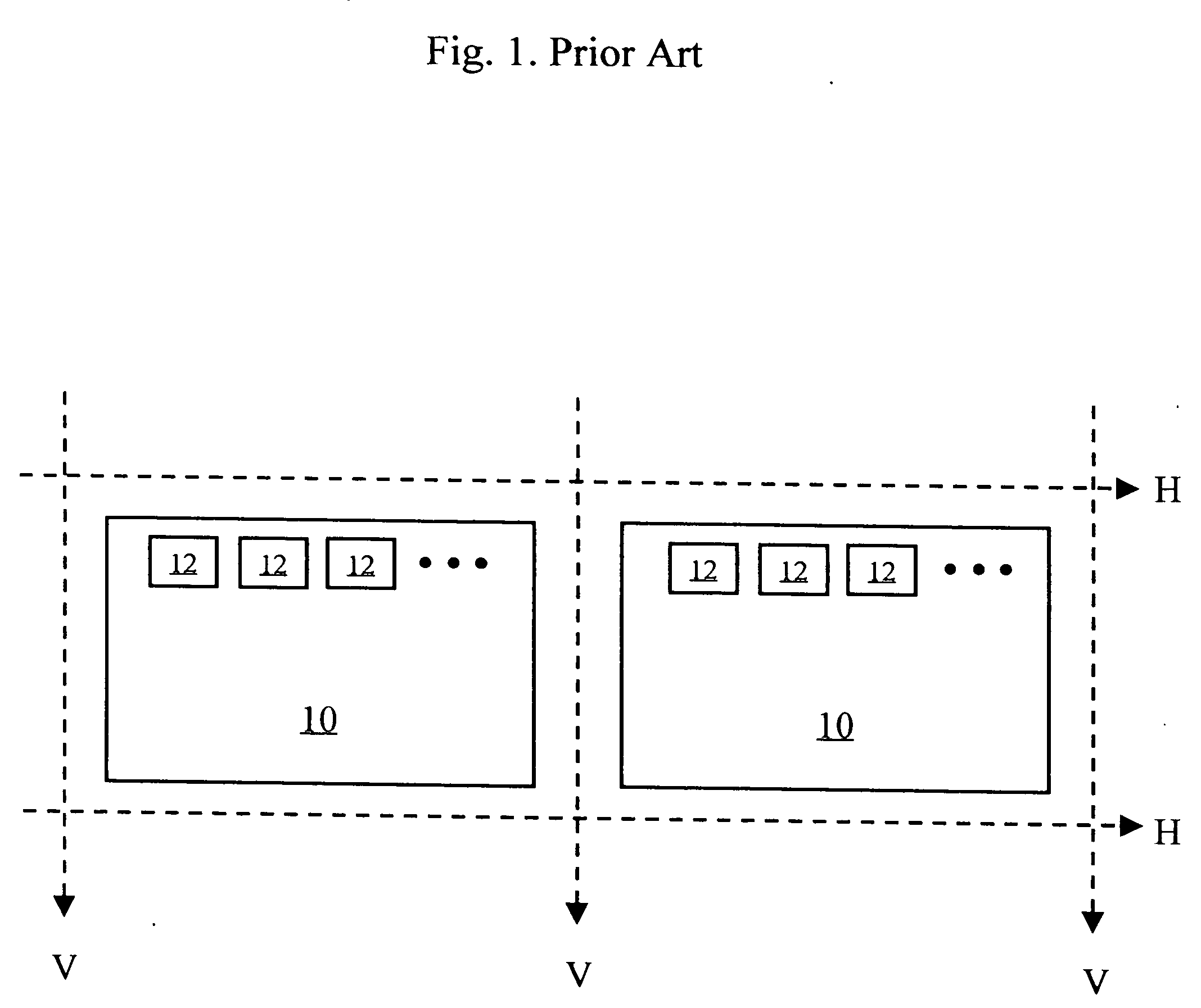
BACKGROUND OF THE INVENTION [0001] 1. Field of the Invention [0002] This invention relates to integrated circuit (IC) memory, particularly to expandable IC memory on the same chip. [0003] 2. Brief Description of Related Art [0004]FIG. 1 shows two adjacent IC memory areas 10 on a common wafer. Each memory area 10 has numerous pads 12 that can be signal pads, power pads, or other functional pads. These pads 12 are used to couple to external circuits. When a customer requests a single capacity memory chip, the wafer is sawed along the horizontal lines H1 and vertical lines V1 to yield single dice each with single capacity memory. When the customer requests double capacity memory, it is necessary that a new product different from the single capacity memory die 10 be redesigned to meet the requirements of double capacity memory. In traditional practice, the double capacity cannot be obtained from combining two of the single capacity memory areas at wafer stage. SUMMARY OF THE INVENTION [...

Claims


Application Information

Patent Timeline
Patent Type & Authority Applications(United States)
IPC IPC(8): G11C8/00
CPCG11C2207/105G11C8/12
Inventor HUNG, CHI-CHENGCHANG, LING-YUEHCHUNG, PWU-YUEH
Owner LYONTEK
Learn More