Transparent Memory for Transparent Electronic Device

a technology of electronic devices and transparent memory, applied in semiconductor devices, digital storage, instruments, etc., can solve the problems of high operating voltage, high power consumption, flash memory, etc., and achieve excellent switching characteristics, high transparency, and maintain the effect of resistive memory

Inactive Publication Date: 2012-05-31
KOREA ADVANCED INST OF SCI & TECH
View PDF1 Cites 43 Cited by
  • Summary
  • Abstract
  • Description
  • Claims
  • Application Information

AI Technical Summary

Benefits of technology

[0028]According to the present invention, there can be provided transparent resistive memory, which has very high transparency, has excellent switching characteristics depending on resistance variations even at a low switching voltage, and is capable of maintaining the switching characteristics of the resistive memory even after a long period of time has elapsed.
[0029]Further, the present invention is advantageous in that when a transparent resistive memory device is manufactured, a substrate can be made of an inexpensive material such as glass, a polymer or plastic, thus reducing manufacturing costs.
[0030]Furthermore, the present invention is configured such that a resistance-variable material layer is formed as a multi-layer, thus increasing memory capacity and improving operating characteristics while reducing the size of the memory.
[0031]Since the above-described transparent resistive memory is not influenced by the size of a substrate when the transparent memory device is manufactured, it can be directly applied to a transparent large-size electronic device.
[0032]Furthermore, since a flexible substrate is used, a transparent electronic device that is not damaged by bending or the like attributable to external force and is flexible and easily portable can be manufactured.

Problems solved by technology

However, DRAM is disadvantageous in that since a capacitor must be continuously recharged with electric charges, power consumption is high, and, in particular, in that DRAM is volatile memory in which all data stored therein is erased when the supply of power to the DRAM is interrupted.
However, flash memory is disadvantageous in that operating voltage is high, and operating speed is much lower than that of DRAM.
Second, there is a switching model based on a large number of traps present in a metal oxide.
Since memory that uses such a substrate is not transparent, it is impossible not only to manufacture a transparent electronic device that can be applied to transparent displays or the like, but also to directly apply electronic devices to transparent electronic products such as large-size transparent displays or the like because memory is influenced by the size of a substrate when being manufactured.

Method used


Image

  • Transparent Memory for Transparent Electronic Device
  • Transparent Memory for Transparent Electronic Device
  • Transparent Memory for Transparent Electronic Device

Examples


Embodiment Construction

[0052]Hereinafter, preferred embodiments of the present invention will be illustrated and referred to so as to describe the present invention, the operating advantages thereof, and objects to be achieved by the implementation of the present invention.

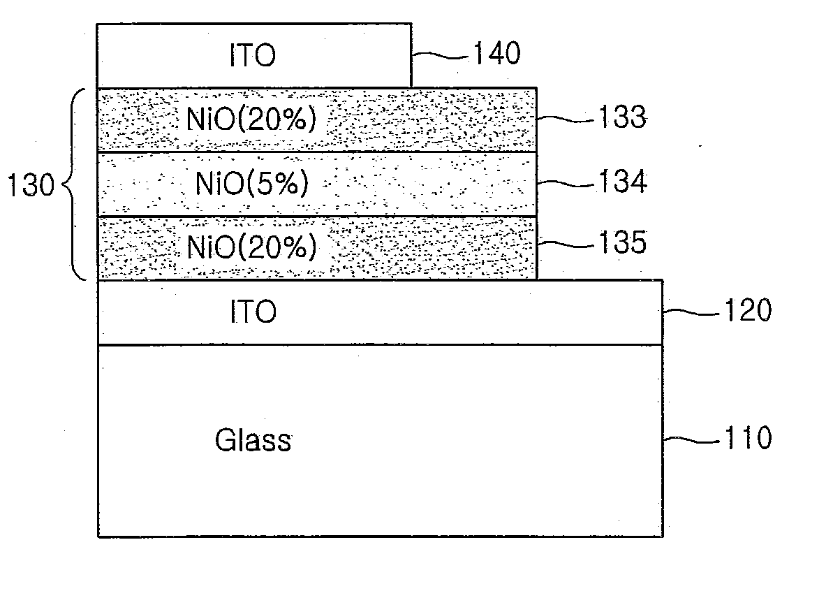
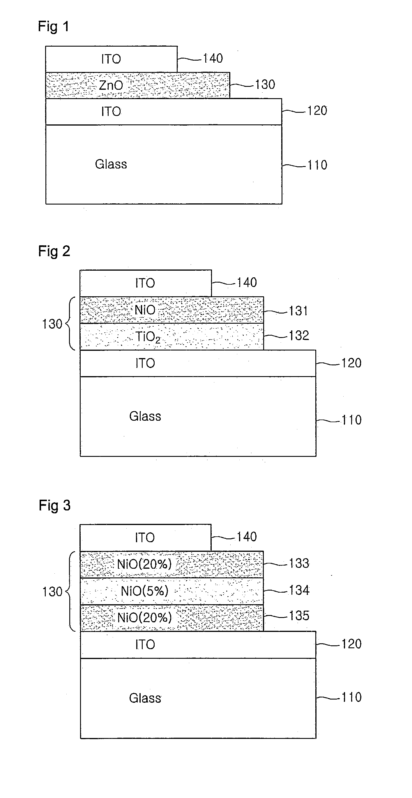
[0053]FIG. 1 is a view showing an embodiment of transparent memory for a transparent electronic device according to the present invention.

[0054]The memory of the present invention includes layers sequentially stacked on a transparent substrate 110, that is, a lower transparent electrode layer 120, a data storage area 130 implemented as a transparent resistance-variable material layer, and an upper transparent electrode layer 140.

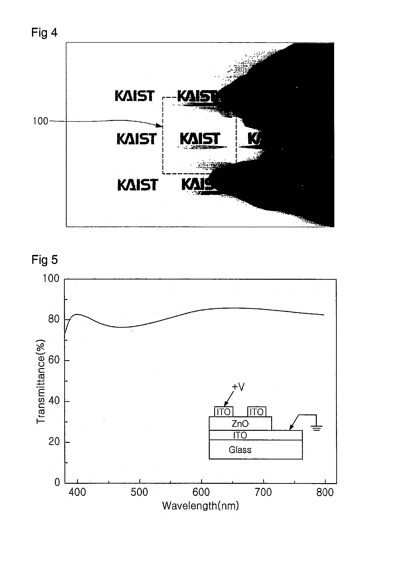
[0055]In the embodiment of FIG. 1, glass is used for the transparent substrate 110, and, in addition to the glass, a polymer or plastic can be used as a transparent insulating material which has a visible light transmittance of 80% or more and does not cause light distortion or refraction.

[0056]Although the tran...


PUM

PropertyMeasurementUnit
visible light transmittanceaaaaaaaaaa
optical band gapaaaaaaaaaa
voltageaaaaaaaaaa

Abstract

The present invention relates to a transparent memory for a transparent electronic device. The transparent memory includes: a lower transparent electrode layer that is sequentially formed on a transparent substrate, and a data storage region and an upper transparent layer which are made of at least one transparent resistance-variable material layer. The transparent resistance-variable material layer has switching characteristics as a result of the resistance variance caused by the application of a certain voltage between the lower and upper transparent electrode layers. An optical band gap of the transparent resistance-variable material layer is 3 eV or more, and transmittivity of the material layer for visible rays is 80% or more. The invention provides transparent and resistance-variable memory that: has very high transparency and switching characteristics depending on resistance variation at a low switching voltage, and can maintain the switching characteristics thereof after a long time elapses.

Description

TECHNICAL FIELD[0001]The present invention relates, in general, to transparent memory for a transparent electronic device and, more particularly, to a transparent memory device, in which transparent electrodes and a transparent resistance-variable material are stacked on a transparent substrate and which realizes high visible light transmittance and obtains excellent switching characteristics, and to transparent memory which is required to apply the transparent memory device to a transparent electronic device.BACKGROUND ART[0002]Generally, semiconductor memory devices are mainly divided into volatile memory and non-volatile memory according to a driving method. Dynamic Random Access Memory (DRAM), which is a representative volatile memory device, includes a single transistor and a single capacitor. Such DRAM is advantageous in that the operating speed thereof is very high, and the degree of integration is also very high, thus enabling large-capacity memory to be implemented. However...

Claims


Application Information

Patent Timeline
Patent Type & Authority Applications(United States)
IPC IPC(8): H01L47/00
CPCH01L21/84H01L27/1203H01L45/00H01L45/146H01L45/1233H01L45/1253H01L45/08H01L27/12G11C13/0007H10B63/30H10B63/84H10N70/20H10N70/823H10N70/826H10N70/841H10N70/8833H10N70/023H10N70/061G11C13/0004
Inventor SEO, JUNG WONLIM, KEONG SUPARK, JAE WOOYANG, JI HWANKANG, SANG JUNG
Owner KOREA ADVANCED INST OF SCI & TECH
Why Eureka
Try Eureka