Memory cell

a memory cell and memory technology, applied in the field of memory cells, can solve the problems of limiting the feature size down scaling, volatile dynamic random access memory devices in the present silicon based technology, and inability to use ram applications, so as to improve the speed of charging and discharging, and remove the problem of down scaling

Inactive Publication Date: 2008-04-22
QS SEMICON AUSTRALIA
View PDF12 Cites 37 Cited by
  • Summary
  • Abstract
  • Description
  • Claims
  • Application Information

AI Technical Summary

Benefits of technology

[0014]One embodiment of the invention is a modification of the 1T flash cell (prior art). The floating gate of the 1T flash cell can be considered as the connection between two capacitor terminals—one capacitor being between the control gate and the floating gate, and the other capacitor being between the floating gate and the channel of the transistor. Then, this embodiment of this invention can simply be described as a replacement of the capacitor on the control-gate side by a SiC diode. The SiC diode can provide the charge retention achieved by the replaced capacitor because both bulk and surface charge generation / recombination are practically negligible in passivated SiC regions. Importantly, the SiC diode can also provide fast and nondestructive charge removal / deposition, avoiding the limitations imposed by the replaced capacitor. Designing the diode as a reference diode enables the use of both forward and reverse turn-on voltages for easier charging and discharging operations. This 1T cell with diode isolation enables straightforward implementation of the architectures used in the present flash memories, and in particular the NOR and the NAND arrays that are established as the industry standards for code and data storage.
[0018]In either embodiment, the cells are read by sensing resistance. This has the consequence of enabling multiple levels with a consequential increase in memory capacity and removes problems in down scaling the cell size.
[0020]Compared to Flash memory lower voltages are required and the speed of charging and discharging is greater than with Flash. The memory cell of this invention has none of the disadvantages of Flash memory with the added benefit that the cell may have several (infinite) logic states if they are needed. Another advantage that this invention has over Flash memory is that in Flash memory charging and discharging is destructive and changes the material state whereas in this invention the passivated interface provides fast and nondestructive charge removal / deposition. In this invention the charging and discharging of the gates through the diode does not change the electrical properties of the material forming the diode and does not in any way stress the gate oxide. With the dynamic memory cell of this invention the number of writing cycles is sufficiently high and the speed of discharging / charging is sufficiently quick to allow for real time data processing. The passivation of the Sic-SiO2 interface creates charge retention times sufficiently long to avoid the need for the memory cell of this invention to be electrically refreshed as is the case with conventional RAM. Charge retention times beyond 7 years are achievable with this invention. Passivation may be by Thermal SiO2 passivation or preferably by nitriding the surface at high temperatures with NO or N2O.
[0022]The fabrication method which results in a self aligned MOSFET with a metal gate provides performance improvements (better down scaling of F, reduced power consumption, and reduced leakage through the gate oxide). Self-aligned MOSFETs are routinely made in silicon (either with polysilicon or metal gates). The challenge in SiC is due to the need for high-temperature annealing to activate the doping of the drain and the source areas after creating them by ion implantation with the MOSFET gates as self-aligning masks. The ion implantation may be performed at room temperature, but this requires prohibitively high annealing temperatures (>1400° C.). An alternative method is to perform the ion-implantation at high temperatures (about 800° C.), in which case the post implant annealing temperature up to 1300° C. is sufficient. The challenge with this is to find a metal (or a metal-based structure) that will provide the necessary adhesion to the gate oxide and that will withstand the high-temperature ion implantation. A preferred metal is Molybdenum and this allows a Mo-gate process that satisfies the conditions for fabrication of self-aligned SiC MOSFETs by hot ion implantation. Other suitable materials are P+ polysilicon, and platinum silicide. An essential feature of this preferred method is the use of a capping dielectric (deposited oxide, for example) to prevent sublimation of the Mo gate, as well as coating the capping dielectric by a thin metal film to avoid damaging charging effects during the ion implantation.
[0041]All these advantages help to achieve higher memory capacities, as evidenced by the fact that higher memory capacities are achieved by modern flash than by modern DRAMs.

Problems solved by technology

Dynamic Random Access Memory devices in the present silicon based technology are volatile because periodic refresh of the stored information is necessary and the information is lost when the memory cells are no longer connected to a power supply.
It is a read-only memory (ROM), because the information writing takes too long and is limited to a certain number of writing cycles, so it cannot be used for RAM applications.
Another challenge in developing memory devices is to enable an increase in memory capacity, and one way of achieving this is to reduce the cell area (8F2 in current DRAMs).
Still, there is a limit to the down scaling of the feature size, set by the need to accelerate electrons to energies that are sufficient for injection into the floating gate.
Silicon Carbide is not widely used to produce semiconductor devices which are mostly fabricated in silicon.

Method used


Image

  • Memory cell
  • Memory cell
  • Memory cell

Examples


Embodiment Construction

[0049]Preferred embodiments of the invention will be described with reference to the drawings in which:

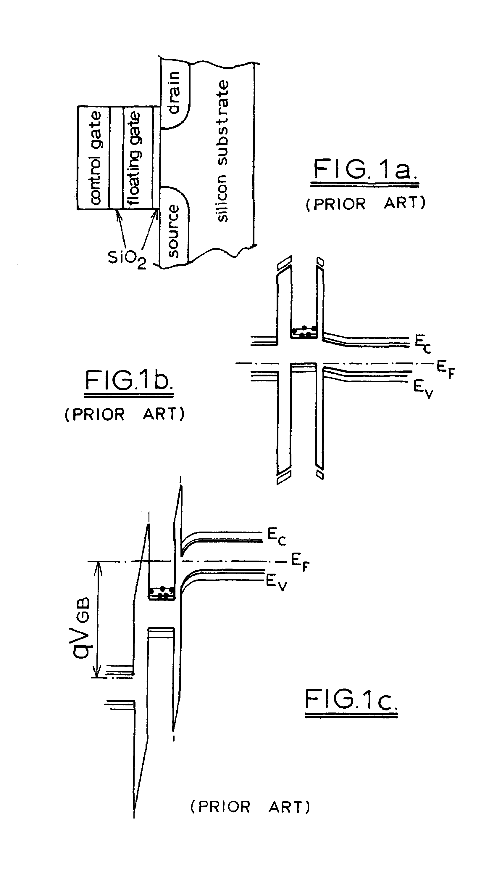
[0050]FIG. 1a-c shows relevant prior art: energy-band diagrams of 1T cell with capacitor-isolated floating gate used in flash memories;

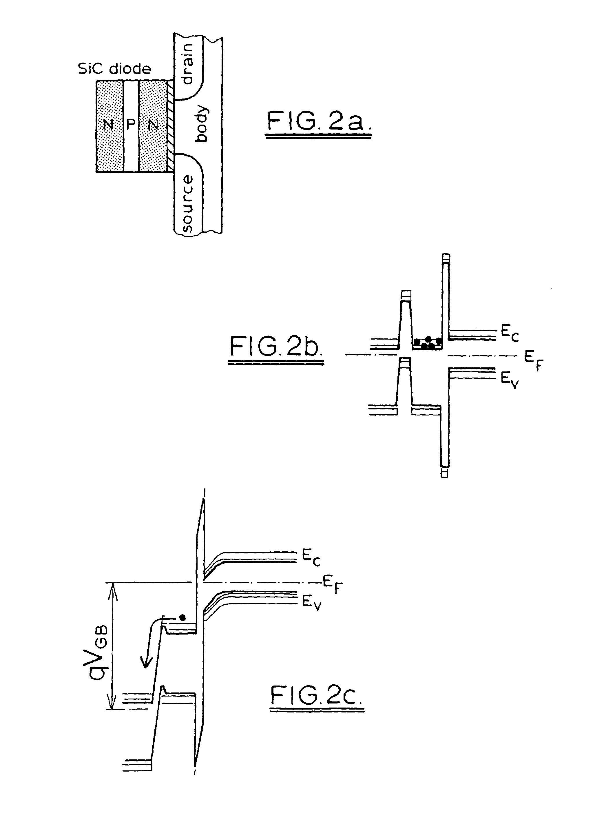
[0051]FIG. 2a-c shows energy-band diagrams of 1T cell with diode isolation disclosed in this invention;

[0052]FIG. 3 is Arrhenius plot of charge-retention times measured at different temperatures with a MOS capacitor on 4H SiC;

[0053]FIG. 4 is Arrhenius plot of charge-retention times measured at different temperatures with a MOS capacitor on 3C SiC;

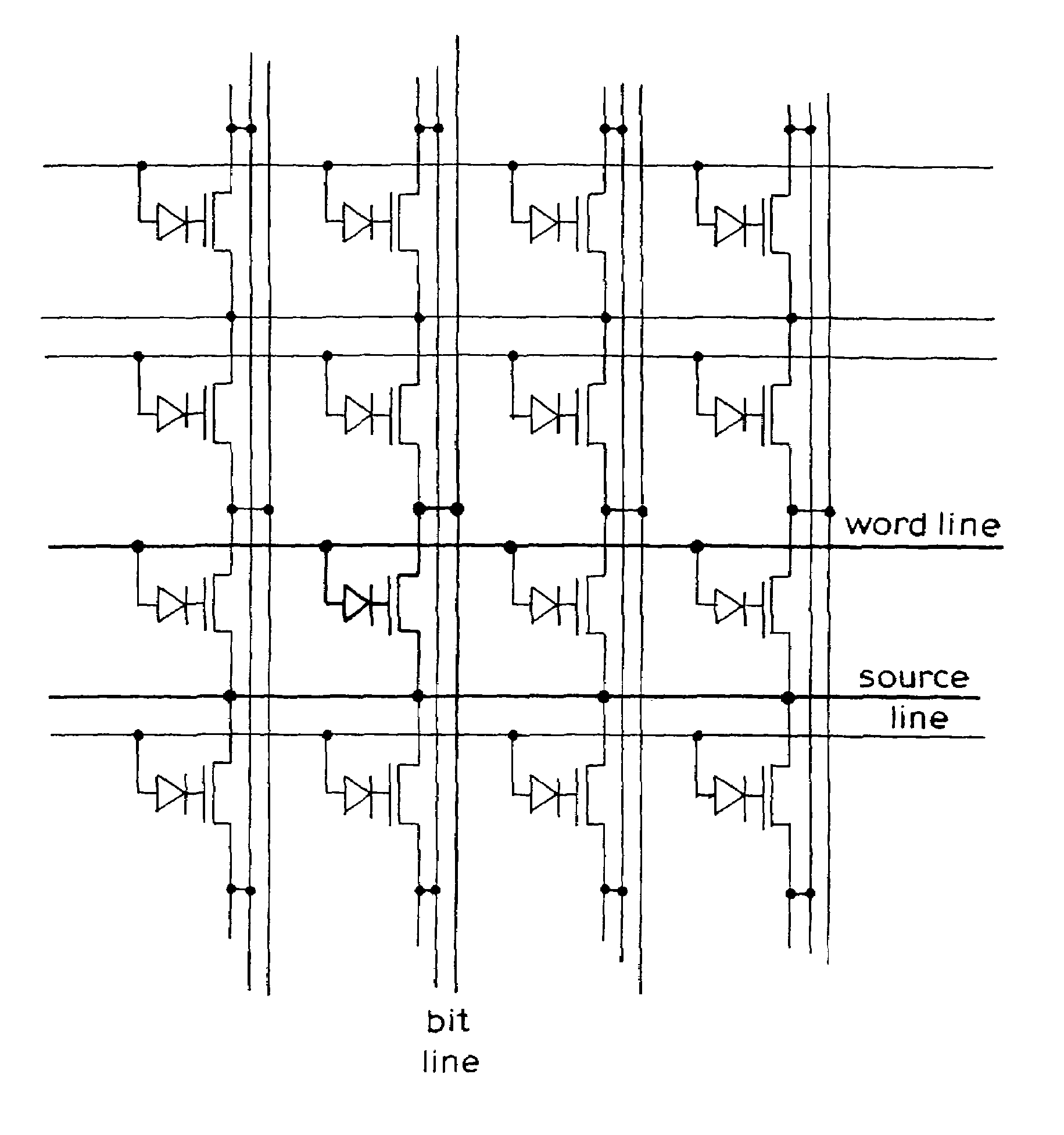
[0054]FIG. 5 is NOR memory array using the 1T cells with diode isolation, disclosed in this invention;

[0055]FIG. 6 is I-V characteristic of a reference diode, defining the forward (VF) and the reverse (VR) turn-on voltages;

[0056]FIG. 7 is cross-sectional view of 1T cells with diode isolation in the preferred implementation;

[0057]FIG. 8 is the layout of 1T cells used in a NOR-type array.

[0058]FIG. 9 is cross...


PUM


Abstract

A one-transistor (1T) NVRAM cell that utilizes silicon carbide (SiC) to provide both isolation of non equilibrium charge, and fast and non destructive charging / discharging. To enable sensing of controlled resistance (and many memory levels) rather than capacitance, the cell incorporates a memory transistor that can be implemented in either silicon or Sic. The 1T cell has diode isolation to enable implementation of the architectures used in the present flash memories, and in particular the NOR and the NAND arrays. The 1T cell with diode isolation is not limited to SiC diodes. The fabrication method includes the step of forming a nitrided silicon oxide gate on the Sic substrate and subsequently carrying out the ion implantation and then finishing the formation of a self aligned MOSFET.

Description

[0001]This invention relates to a nonvolatile memory cell and in particular to a silicon carbide based memory cell.BACKGROUND TO THE INVENTION[0002]Dynamic Random Access Memory devices in the present silicon based technology are volatile because periodic refresh of the stored information is necessary and the information is lost when the memory cells are no longer connected to a power supply.[0003]Flash memory provides the complementary functions in modern electronic systems. Flash memory uses a floating gate which is charged or discharged through the surrounding insulating material to change the logic state. It is a read-only memory (ROM), because the information writing takes too long and is limited to a certain number of writing cycles, so it cannot be used for RAM applications. However, it provides a nonvolatile storage of the information, which is kept even when any power is disconnected from the memory cells. Flash memory is also dependent on processing and in practice there is...

Claims


Application Information

Patent Timeline
Patent Type & Authority Patents(United States)
IPC IPC(8): G11C11/36G11C16/04H01L21/82H01L21/8242H01L21/8247H01L27/10H01L27/108H01L27/115
CPCG11C16/04H01L27/11521H01L27/115H01L21/8213H10B69/00H10B41/30H10B63/20
Inventor HARRISON, BARRY H.DIMITRIJEV, SIMA
Owner QS SEMICON AUSTRALIA
Why Eureka
Try Eureka